Failure analysis device and analysis method for tsv wafer level package mems chip

A technology of wafer-level packaging and failure analysis, which is applied in the field of MEMS chip analysis, can solve problems such as the inability to use the response of the MEMS structure 21a with the cover removed, and achieve simple structure, accurate failure analysis, and good results

Active Publication Date: 2016-09-21
ANHUI BEIFANG XINDONG LIANKE MICROSYST TECH
View PDF6 Cites 0 Cited by
  • Summary
  • Abstract
  • Description
  • Claims
  • Application Information

AI Technical Summary

Problems solved by technology

The bonding pad 29 of the MEMS chip of this TSV wafer level package is positioned at the top of the cover plate 26. After the cover plate 26 is removed, the bonding pad 29 and the MEMS structure 21a are distributed on the upper and lower sides of the cover plate 26. Like this, in failure analysis When the cover plate is removed, the response of the MEMS structure 21a cannot be directly observed through a microscope. Therefore, for MEMS chips in TSV wafer-level packaging, how to perform failure analysis has become a difficult problem at present.

Method used


Image

  • Failure analysis device and analysis method for tsv wafer level package mems chip
  • Failure analysis device and analysis method for tsv wafer level package mems chip
  • Failure analysis device and analysis method for tsv wafer level package mems chip

Examples


Embodiment 1

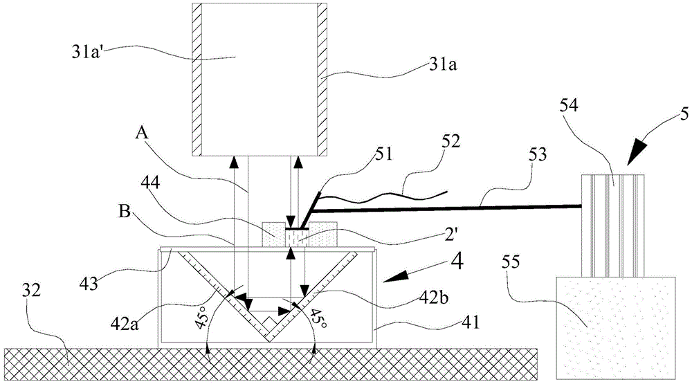
[0039] TSV wafer-level packaging MEMS chip failure analysis device such as image 3 , Figure 4 As shown, it is composed of a microscope, a reflector box 4 and a probe system 5;

[0040] The microscope comes with a light source with a small-magnification objective lens 31a, a large-magnification objective lens 31b and a movable stage 32 for observing the MEMS structure 21a of the MEMS chip 2'to be analyzed and its movement;

[0041] The function of the reflector box 4 is to reflect light and carry the MEMS chip 2'to be analyzed. It is composed of an open top shell 41, a reflector, transparent glass 43, and a pair of positioning blocks 44 for fixing the MEMS chip 2'to be analyzed. The reflector includes Two left reflector 42a and right reflector 42b that form a 90° angle to each other. The left reflector 42a and the right reflector 42b are mounted in the housing 41 with their mirror surfaces facing upward. The left reflector 42a and the right reflector 42b are connected to the housin...

Embodiment 2

[0047] The failure analysis device of the TSV wafer-level package MEMS chip of this embodiment is different from the failure analysis device of the TSV wafer-level package MEMS chip of the first embodiment only in that the MEMS chip to be analyzed 2" is placed on the upper surface of the transparent glass 43. There is a cavity 43a at the position, such as Image 6 Shown. Since the MEMS chip 2" to be analyzed has no sealing layer 22 and cannot be directly placed on the transparent glass 43, a cavity 43a needs to be made on the transparent glass 43, so that when the MEMS chip 2" to be analyzed is placed, the MEMS sealing area 21b and When the transparent glass 43 is in contact, the MEMS structure 21a is located in the cavity 43a and can move freely, which solves the problem that the MEMS chip 2" cannot move after the probe 51 is stuck on the pressure pad 29 in Example 1.

Embodiment 3

[0049] TSV wafer-level packaging MEMS chip failure analysis device such as Figure 7 As shown, it is composed of a microscope, a reflector box 4 and a probe system 5;

[0050] The microscope comes with a light source, an objective lens 31 and a movable stage 32 for observing the MEMS structure 21a of the MEMS chip 2" to be analyzed and its movement;

[0051] The function of the reflector box 4 is to reflect light and carry the MEMS chip 2" to be analyzed. It is composed of a shell 41 with an opening at the top, a reflector and a transparent glass 43. The reflector includes two left reflectors 42a and a right reflector with a 90° angle to each other. The mirror 42b, the left reflector 42a and the right reflector 42b are all mounted in the housing 41 with the mirror surface facing upwards. The left reflector 42a and the right reflector 42b and the bottom surface of the housing 41 have an angle of 45°, and the transparent glass 43 covers the housing. At the top opening of 41, the tran...


PUM


Abstract

The invention discloses a device and a method for analyzing failures of TSV (through silicon via) wafer level packaged MEMS (micro-electro-mechanical systems) chips. The device comprises a microscope, a reflective box and a probe system. The reflective box comprises a shell, two reflective mirrors and transparent glass, a 90-degree angle is formed by the two reflective mirrors in the shell, the transparent glass is arranged at a top opening of the shell, and 45-degree included angles are formed between the reflective mirrors and the bottom of the shell; the probe system comprises probes, probe arms and a probe seat, the probes are connected with the probe seat by the probe arms, and conducting wires are connected onto the probes and are connected with testing devices or power sources. The method includes placing a to-be-analyzed MEMS chip on the transparent glass and pricking the probes on a pressure welding block; inputting excitation voltages into an MEMS structure via the conducting wires; observing response of the MEMS structure via the microscope and judging failure mechanisms of an MEMS device. The device and the method have the advantages that the directions of light rays can be changed by the aid of the reflective mirrors, the failure mechanisms of the MEMS chip can be analyzed without back lenses, the device is simple in structure, and good effects can be realized by the device; the method is simple in operation, and the failures of the to-be-analyzed MEMS chip can be quickly and accurately analyzed by the aid of the method.

Description

Technical field [0001] The invention belongs to the field of MEMS chip analysis, and specifically relates to a failure analysis device for TSV wafer-level packaging MEMS chips. The invention also relates to a method for performing failure analysis of MEMS chips by using this analysis device. Background technique [0002] MEMS (Micro-Electro-Mechanical Systems) is the abbreviation of Micro-Electro-Mechanical Systems. MEMS manufacturing technology uses micro-machining technology, especially semiconductor wafer manufacturing technology, to create various micro-mechanical structures, combined with application-specific control integrated circuits (ASIC), to form Intelligent micro sensors, micro actuators and other MEMS components. MEMS components have the advantages of small size, low cost, high reliability, strong resistance to harsh environments, low power consumption, high intelligence, easy calibration, and easy integration. They are widely used in consumer electronic products (su...

Claims


Application Information

Patent Timeline
Patent Type & Authority Patents(China)
IPC IPC(8): H01L21/66
CPCB81C99/004B81C99/005
Inventor 华亚平
Owner ANHUI BEIFANG XINDONG LIANKE MICROSYST TECH
Why Eureka
Try Eureka