Apparatus for backside EMMI failure analysis and failure analysis method thereof

A failure analysis, backside technology, used in electronic circuit testing, optical testing flaws/defects, non-contact circuit testing, etc., can solve problems such as poor repeatability, difficulty, and difficult operation, and achieve high repeatability.

Inactive Publication Date: 2013-11-13
SHANGHAI HUAHONG GRACE SEMICON MFG CORP
View PDF4 Cites 4 Cited by
  • Summary
  • Abstract
  • Description
  • Claims
  • Application Information

AI Technical Summary

Problems solved by technology

[0008] Due to space limitations, it is impossible to have too many probes, and generally only 5 to 6 pins can be connected; at the same time, the area of ​​the contact point between the probe and the metal wire is small and not fixed, so it is necessary to balance 5 to 6 pins. 6 needles, it is very difficult to ensure good contact at the same time, it takes a long time, the operation is difficult, and the repeatability is poor
Moreover, due to the limitation of probes, most of the test functions that require multiple signal control are greatly limited
[0009] In addition, this backside EMMI failure analysis method is only applicable to packaged products, and it takes several working days to complete the precise location of a single defect area, especially when multiple signal inputs are required
In the context of the current rapid development of semiconductor technology, the continuous reduction of device feature size, and the continuous rise of integration, this failure analysis method is not acceptable due to time delays and signal input limitations. The analysis of the mechanism poses great challenges

Method used


Image

  • Apparatus for backside EMMI failure analysis and failure analysis method thereof
  • Apparatus for backside EMMI failure analysis and failure analysis method thereof
  • Apparatus for backside EMMI failure analysis and failure analysis method thereof

Examples


Embodiment Construction

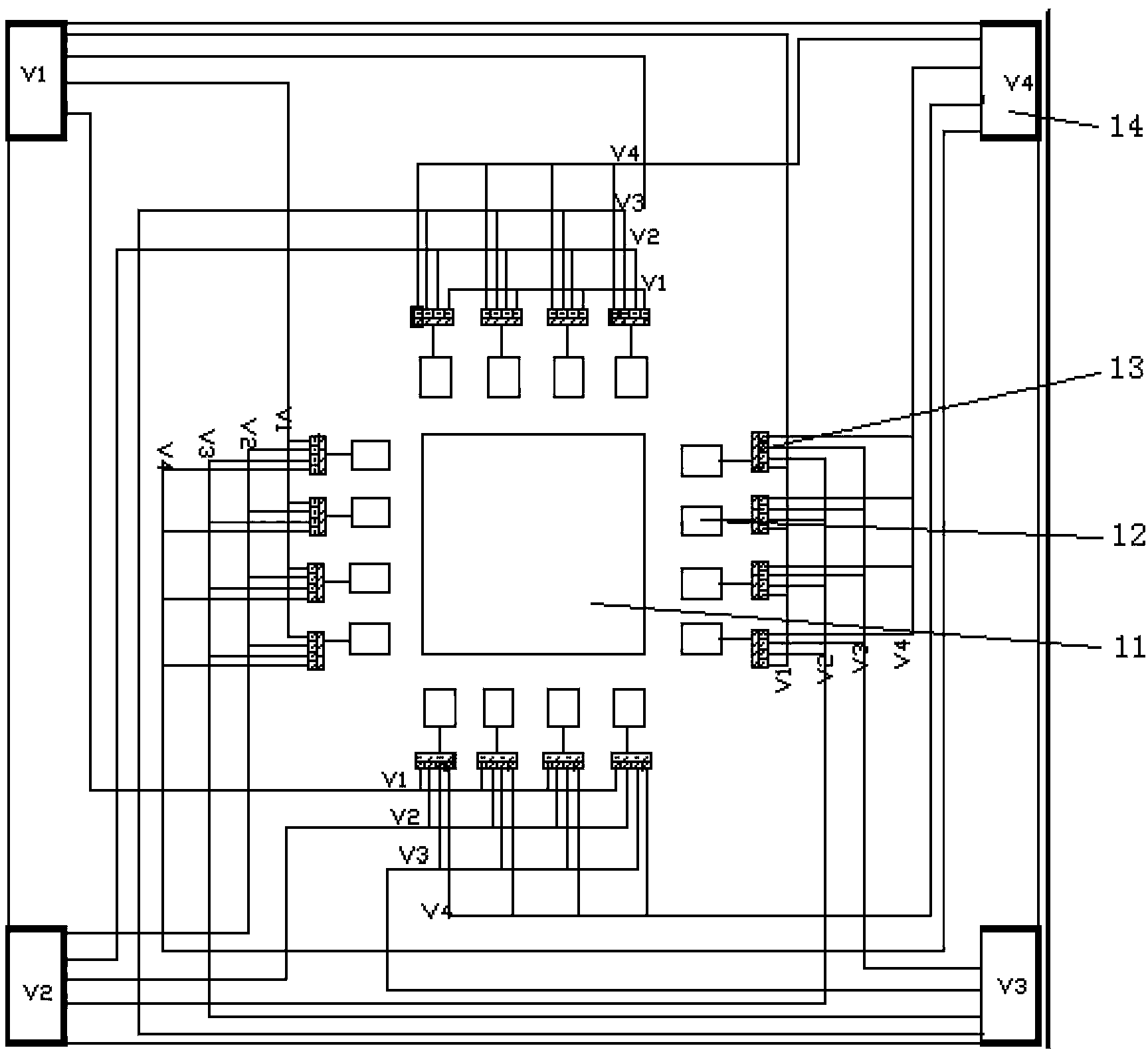
[0038] The device for EMMI failure analysis on the back side of the present invention includes a PVC (Polyvinyl chloride resin polyvinyl chloride) circuit board and a signal input and output base for fixing; the signal input and output base can conduct signals;

[0039] Such as image 3 As shown, the center of the PVC circuit board is provided with a transparent plexiglass sheet 11; the plexiglass sheet 11 is used to position the bare chip, and will not block the EMMI to capture the infrared spectrum;

[0040] On the front side of the PVC circuit board, a plurality of metal pins 12 are arranged around the plexiglass sheet 11; four on each side have a total of sixteen metal pins 12; each metal pin 12 can be connected to at least six bare chip pins ;

[0041] The four corners of the PVC circuit board are respectively provided with circuit board metal pads (pads) 14;

[0042] Each metal pin 12 is connected to a jumper interface 13 by metal wire respectively, and each jumper int...


PUM


Abstract

The invention discloses an apparatus for the backside EMMI failure analysis. The apparatus comprises a PVC circuit board and a signal input and output pedestal; a transparent synthetic glass sheet is arranged in the center of the PVC circuit board, and a plurality of metal pins are arranged in the periphery of the synthetic glass sheet; circuit board metal pads are arranged at the four corners of the PVC circuit board respectively; each of the metal pins is connected with a jumper wire interface through a metal wire, and the jumper wire interface is connected with the four circuit board metal pads through metal wires respectively; and the signal input and output pedestal comprises a pedestal body, pedestal metal pads are arranged at the four corners of the pedestal body respectively, and the positions of the pedestal metal pads correspond to the positions of the circuit board metal pads. The apparatus allows the backside EMMI failure analysis to simply, rapidly and reliably realize the failure point positioning, and the positioning time of failure defects to be shortened to several hours from original several days. The invention also discloses a method for the backside EMMI failure analysis.

Description

technical field [0001] The invention relates to a failure analysis equipment of a semiconductor device, in particular to a device for failure analysis of backside EMMI. The invention also relates to a backside EMMI failure analysis method. Background technique [0002] For semiconductor failure analysis (FA), infrared emission microscope (IR Emission Microscope, EMMI) is a very efficient defect localization analysis tool, which can capture the photons emitted by electron-hole recombination in semiconductor components, The detectable wavelength is about 350-1100nm. Therefore, EMMI (luminescent microscope) can be widely used to detect leakage currents generated by various component defects in IC (semiconductor), such as Gate oxide defects (gate oxide defects), Leakage defects (leakage defects), Latch up (gate lock) , ESD failure (electrostatic failure), etc. [0003] Because most of the defects in IC devices show weak luminescence when the chip is working, EMMI can locate t...

Claims


Application Information

Patent Timeline
Patent Type & Authority Applications(China)
IPC IPC(8): G01N21/88G01R31/308
Inventor 蔡妮妮方昭蒂范加森
Owner SHANGHAI HUAHONG GRACE SEMICON MFG CORP
Why Eureka
Try Eureka