A method for measuring carrier concentration in solar-grade monocrystalline silicon

A carrier concentration, solar-level technology, applied in the direction of measuring devices, single semiconductor device testing, instruments, etc., can solve the problem of carrier mobility decline, achieve simple and fast measurement, reduce test cost, and high practical value Effect

Inactive Publication Date: 2017-06-20
ZHEJIANG UNIV
View PDF4 Cites 0 Cited by
  • Summary
  • Abstract
  • Description
  • Claims
  • Application Information

AI Technical Summary

Problems solved by technology

For example, the silicon raw material purified by physical metallurgy contains high concentrations of impurities such as boron and phosphorus at the same time. There is a boron and phosphorus compensation effect in crystalline silicon grown using this raw material. This effect is first manifested in the high concentration of boron and phosphorus impurities. leading to a decrease in carrier mobility

Method used


Image

  • A method for measuring carrier concentration in solar-grade monocrystalline silicon
  • A method for measuring carrier concentration in solar-grade monocrystalline silicon
  • A method for measuring carrier concentration in solar-grade monocrystalline silicon

Examples


Embodiment 1

[0051] (1) Select a series of p-type electronic grade single crystal silicon as standard samples, the resistivity of the standard sample is 0.05-50Ω·cm, and the resistivity of the standard sample is evenly distributed in each resistivity range. The thickness of the standard sample is uniform, 1-2mm.

[0052] (2) After the standard samples are cleaned by the standard cleaning process, the resistivity of each sample is measured at room temperature according to the national standard "Method for Measuring the Resistivity of Silicon Single Crystal" (GB / T 1551-2009), and the resistance of each sample is measured by formula (5) The rate is converted to the corresponding carrier concentration.

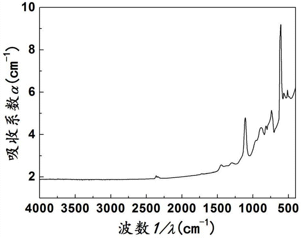
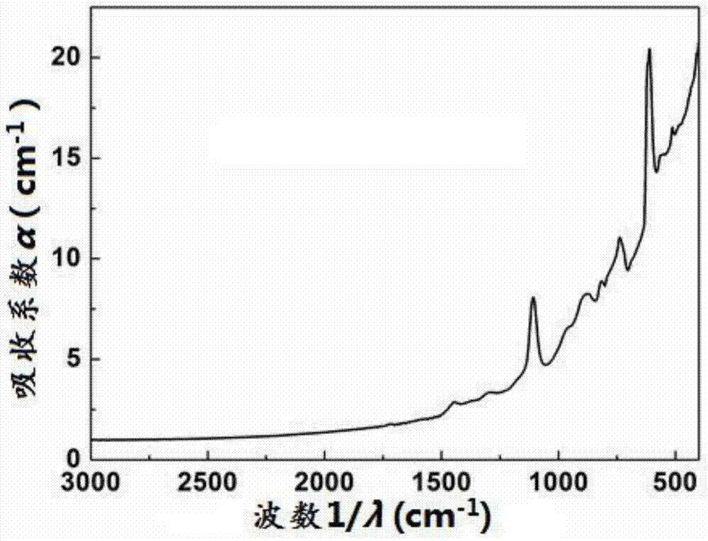
[0053] (3) The standard sample is chemically polished to make the two surfaces mirror-like, and after cleaning by standard cleaning process, the infrared transmission coefficient of each sample is measured by the Fourier Transform Infrared Spectrometer (FTIR) and converted into infrared by formula ...

Embodiment 2

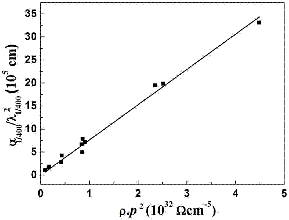
[0061] Steps (1) to (3) are the same as in Example 1. In step (4), the (α) of p-type single crystal silicon λ1 -α λ2 ) / (λ 1 2 -λ 2 2 ) And ρp 2 The standard curve, where: λ 1 = 1 / 400cm, λ 2 =1 / 1150cm, α λ1 With α λ2 Respectively wavelength λ 1 , Λ 2 The infrared absorption coefficient of the standard sample, such as Figure 4 As shown, the expression is: (α λ1 -α λ2 ) / (λ 1 2 -λ 2 2 )=(α 1 / 400 -α 1 / 1150 ) / (λ 2 1 / 400 - / λ 2 1 / 1150 )=7.9×10 -27 ρp (9)

[0062] For a certain boron-phosphorus-compensated solar-grade monocrystalline silicon sample to be tested in Example 1, the carrier concentration calculated according to formula (9) is 2.63×10 16 cm -3 . As a preferred method, the result is more accurate than Example 1.

[0063] It can be seen that the method of the present invention can be used to accurately measure the carrier concentration in solar-grade monocrystalline silicon.


PUM

PropertyMeasurementUnit
electrical resistivityaaaaaaaaaa
thicknessaaaaaaaaaa
electrical resistivityaaaaaaaaaa

Abstract

The invention discloses a method for measuring carrier concentration in solar-grade monocrystalline silicon, which comprises the following steps: (1) respectively selecting a series of p-type and n-type electronic-grade monocrystalline silicon as standard samples, and separately Measure its resistivity and infrared absorption coefficient, and convert it into the corresponding carrier concentration according to its resistivity; (2) According to the measurement results of step (1), respectively establish the α of p-type and n-type single crystal silicon λ / λ 2 with ρp 2 The standard curve of , where: α λ is the infrared absorption coefficient of the standard sample under the wavelength λ, p and ρ are the corresponding carrier concentration and resistivity respectively; Measure its resistivity and infrared absorption coefficient, and obtain the carrier concentration according to the corresponding standard curve in step (2). The method is simple and fast, has high precision and low test cost, and is especially suitable for solar-grade monocrystalline silicon with compensation effects in the matrix.

Description

Technical field [0001] The invention relates to the detection of characteristic parameters of semiconductor materials, in particular to a method for measuring the concentration of carriers in solar-grade monocrystalline silicon. Background technique [0002] The electrons and holes that can conduct electricity in semiconductor materials are called carriers. The carrier concentration is the basic parameter of optoelectronic materials and has an extremely important impact on electrical properties. In semiconductor materials, the carrier concentration in the material is often controlled by controlling the type and concentration of doped impurities, and ultimately the purpose of controlling the electrical properties of the material is achieved. Solar-grade semiconductor materials have high requirements for material purity, carrier mobility, and light absorption coefficient. Monitoring and controlling the concentration and distribution of carriers in semiconductors is a key point in ...

Claims


Application Information

Patent Timeline
Patent Type & Authority Patents(China)
IPC IPC(8): G01R31/26G01N27/04G01N21/3563
Inventor 余学功陈鹏杨德仁
Owner ZHEJIANG UNIV
Why Eureka
Try Eureka