Electrode structure of LED chip with conductive substrate

A technology of LED chips and conductive substrates, applied in circuits, electrical components, semiconductor devices, etc., can solve the problems of reducing the service life of the chip, heat accumulation of the chip, shading of the light-emitting area of ​​the chip, etc., to delay the decay of the chip, improve the life of the chip, The effect of reducing heat build-up

Active Publication Date: 2014-11-19
浙江老鹰半导体技术有限公司
View PDF5 Cites 3 Cited by
  • Summary
  • Abstract
  • Description
  • Claims
  • Application Information

AI Technical Summary

Problems solved by technology

It can be seen that the existing LED chips need to make electrodes on the light-emitting surface, which shields the light-emitting area of ​​the chip to varying degrees, cannot fully utilize the entire light-emitting area of ​​the chip, and ha

Method used


Image

  • Electrode structure of LED chip with conductive substrate
  • Electrode structure of LED chip with conductive substrate
  • Electrode structure of LED chip with conductive substrate

Examples


Example Embodiment

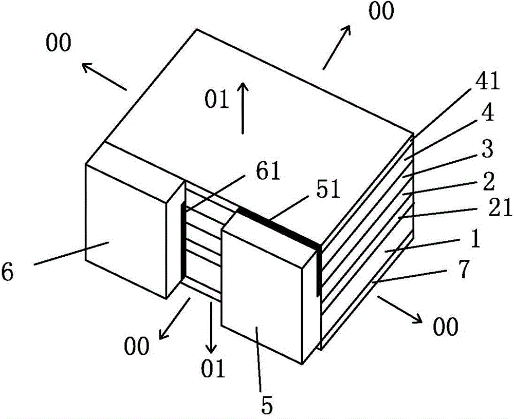
[0016] The present invention will be described in further detail below in conjunction with the accompanying drawings and embodiments. The invention can be implemented at least on LED chips with non-conductive substrates, LED chips with conductive substrates and LED chips without substrates. Unless otherwise specified, within the knowledge of those skilled in the art, the electrode structure described below for a certain type of chip is universal for other types of chips.

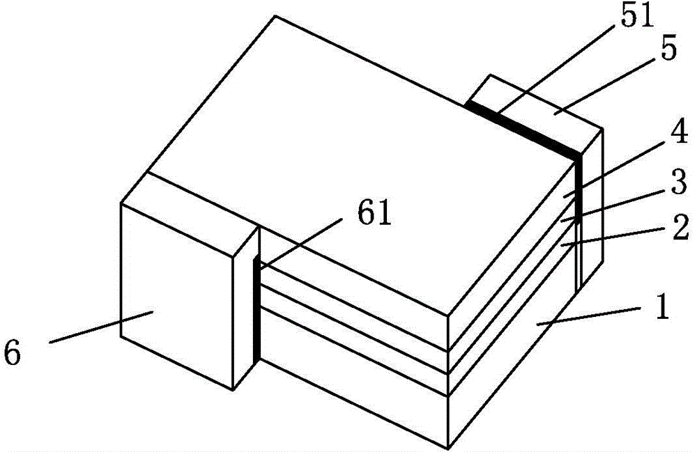
[0017] refer to figure 1 , taking a chip structure with a non-conductive dielectric sapphire as an example, there are substrate 1, N-type semiconductor layer 2, light-emitting layer 3 and P-type semiconductor layer 4 from bottom to top. The chip is cut into a hexahedral structure. The surfaces on the sapphire substrate 1 side of the chip and the two sides of the P-type semiconductor layer 4 are the light-emitting surface 01 of the chip, and the remaining four surfaces located on the side of the light-emitti...


PUM


Abstract

The invention provides an electrode structure of an LED chip with a conductive substrate. The electrode structure comprises a conductive substrate, an N-type semi-conductor layer lapped on the conductive substrate, an emitting layer lapped on the N-type semi-conductor layer and a P-type semi-conductor layer lapped on the emitting layer, wherein the surface on the conductive substrate side of the chip and the surface on the side of the P-type semi-conductor layer are the light-emitting surfaces of the chip, and the other surfaces positioned on the side edges of the light-emitting surface are the side surfaces of the chip; a P-type electrode in electric contact with the P-type semi-conductor layer is arranged on each the side surface; an insulating layer is arranged between each of the P-type electrode and the side surface of the emitting layer, and between the P-type electrode and the side surface of the N-type semi-conductor layer. According to the electrode structure, since the electrodes are arranged on the side surfaces of the chip, the light-emitting area of the chip is enlarged, and brightness of the chip is improved.

Description

technical field [0001] The invention relates to an LED chip structure, in particular to a structure for electrode arrangement on the LED chip. Background technique [0002] According to the different conductive properties of the substrate, the existing LED chips are generally divided into non-conductive substrate chips and conductive substrate chips. Silicon substrates, silicon substrates and gallium nitride substrate chips, etc., are also called vertical structure chips or single-electrode chips. The P-type electrode of the front-mounted chip can be directly fabricated on the P-type semiconductor layer, but because the sapphire substrate carrying the N-type semiconductor layer does not have a conductive function, when making the N-type electrode, it is necessary to cut out some areas on the P-type semiconductor surface until the N-type semiconductor layer is exposed, and then make an N-type electrode on the exposed N-type semiconductor layer. Calculated on a chip with a s...

Claims


Application Information

Patent Timeline
IPC IPC(8): H01L33/36H01L33/48
CPCH01L33/385
Inventor 李媛
Owner 浙江老鹰半导体技术有限公司
Why Eureka
Try Eureka