Supercharge Your Innovation With Domain-Expert AI Agents!

optical communication device

A technology of optical communication and light concentrating device, applied in the field of optical communication, can solve the problems of unfavorable miniaturization, large volume of optical coupling shell, increase the volume of optical communication device, etc., and achieve the effect of being beneficial to miniaturization and reducing volume

Inactive Publication Date: 2017-07-11
SCIENBIZIP CONSULTINGSHENZHENCO
View PDF7 Cites 0 Cited by
  • Summary
  • Abstract
  • Description
  • Claims
  • Application Information

AI Technical Summary

Problems solved by technology

However, since the two optical coupling shells cover the light-emitting element and the light-receiving element, the planar optical waveguide usually needs to be thicker or a cushion layer is provided between the planar optical waveguide and the circuit board, such as the planar optical waveguide to be compatible with the two optical The coupling shell is used for optical coupling, which increases the volume of the optical communication device
In addition, the volume of the optical coupling housing is usually large, which also increases the volume of the optical communication device, which is not conducive to miniaturization

Method used


Image

  • optical communication device

Examples


Embodiment Construction

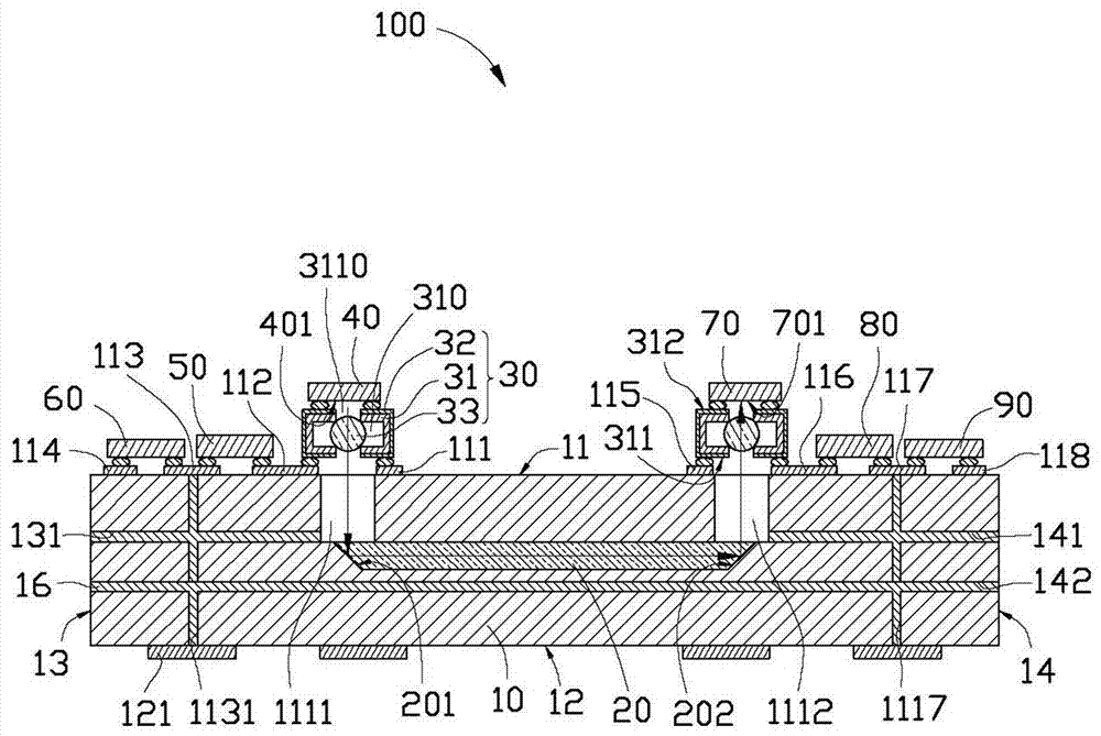
[0051] Such as figure 1 As shown, an optical communication device 100 provided by an embodiment of the present invention includes a circuit board 10, a planar optical waveguide 20, two concentrating devices 30, a light emitting element 40, a first controller 50, and a processing device 60, a light receiving element 70, a second controller 80, and a memory 90.

[0052] In this embodiment, the circuit board 10 is a multi-layer circuit board made of silicon material, which includes a mounting surface 11, a lower surface 12 opposite to the mounting surface 11, a first side 13 and a A second side 14 opposite to the first side 13 . In this embodiment, the installation surface 11 is substantially parallel to the lower surface 12 , and the first side surface 13 is substantially parallel to the second side surface 14 . Both the first side 13 and the second side 14 are vertically connected to the installation surface 11 and the lower surface 12 .

[0053] Four welding pads are formed...


PUM


Abstract

An optical communication device includes a planar optical waveguide, a circuit board, a light-emitting element and a light-receiving element. The circuit board includes a mounting surface. Both the light-emitting element and the light-receiving element are carried on the mounting surface, and both are electrically connected to the circuit board. The light emitting element includes a light emitting surface. The light receiving surface includes a light receiving surface. The planar optical waveguide is embedded in the circuit board, and the planar optical waveguide includes a first inclined surface inclined relative to the installation surface and a second inclined surface inclined relative to the installation surface. A first light guide hole and a second light guide hole are defined on the installation surface. The first slope communicates with the first light guide hole. The second slope communicates with the second light guide hole. The light-emitting surface is opposite to the first slope through the first light guide hole. The light receiving surface is opposite to the second slope through the second light guide hole. The optical communication device is small in size.

Description

technical field [0001] The present invention relates to the field of optical communication, in particular to an optical communication device. Background technique [0002] Existing optical communication devices generally include a circuit board, a light emitting element, a light receiving element, a planar light wave circuit (PLC) and two optical coupling housings. The light-emitting element and the light-receiving element are arranged on the circuit board at intervals. The planar optical waveguide is formed on the circuit board and arranged between the light-emitting element and the light-receiving element. Two optical coupling shells cover the light-emitting element and the light-receiving element respectively, one of which is coupled with one end of the light-emitting element and the planar optical waveguide, and the other optical coupling shell is coupled with the other end of the light-receiving element and the planar optical waveguide coupling. However, since the tw...

Claims


Application Information

Patent Timeline
Patent Type & Authority Patents(China)
IPC IPC(8): G02B6/42
Inventor 曾国峰
Owner SCIENBIZIP CONSULTINGSHENZHENCO
Features
  • R&D
  • Intellectual Property
  • Life Sciences
  • Materials
  • Tech Scout
  • Unparalleled Data Quality
  • Higher Quality Content
  • 60% Fewer Hallucinations
Learn More