
Liquid crystal display panel, display device and method for manufacturing liquid crystal display panel

A technology of a liquid crystal panel and a manufacturing method, which are applied in the manufacture of display devices and liquid crystal panels, and the field of liquid crystal panels, can solve the problems of complex manufacturing process, high manufacturing difficulty and high technological difficulty, and achieve simplified manufacturing process, great manufacturing difficulty and high manufacturing process. simple effect

Active Publication Date: 2014-11-26
BOE TECH GRP CO LTD +1
View PDF8 Cites 5 Cited by
  • Summary
  • Abstract
  • Description
  • Claims
  • Application Information

AI Technical Summary

Problems solved by technology

However, this method needs to rub the alignment layer multiple times in one pixel, and the manufacturing process is complicated. In addition, it is difficult to manufacture a rubbing roller that rubs multiple times in the same pixel area, which makes the process difficult and difficult to realize.

Method used


Image

  • Liquid crystal display panel, display device and method for manufacturing liquid crystal display panel
  • Liquid crystal display panel, display device and method for manufacturing liquid crystal display panel
  • Liquid crystal display panel, display device and method for manufacturing liquid crystal display panel

Examples


Embodiment 1

[0129] Siloxane side chain liquid crystal monomer Y 1 use Figure 5 The siloxane side chain liquid crystal elastomer shown, wherein m=4, n=3, k=3, the crosslinking agent shown in formula II (n=3 in formula II) and the liquid crystallinity shown in formula I The monomers (k=3 in formula I) are grafted in a molar ratio of 1:6. Siloxane side chain liquid crystal monomer Y 1 Helical Twisting Power (HTP for short, the unit is μm -1 ) with temperature (Temperature, unit is ℃) change curve as shown in Figure 15 As shown, its pitch at 70°C is 240nm. Using this siloxane side chain liquid crystal elastomer Y 1 As the second alignment layer, it can be combined with the first alignment layer to form an initial arrangement of multiple liquid crystal molecules in one pixel to realize multi-domain liquid crystal display, including siloxane side chain liquid crystal elastomer Y 1 The production steps of the LCD panel are as follows:

[0130] Form a first alignment layer aligned along ...

Embodiment 2

[0137] Siloxane side chain liquid crystal monomer Y 1 use Figure 5 The siloxane side chain liquid crystal elastomer shown, wherein m=4, n=3, k=3, the crosslinking agent shown in formula II (n=3 in formula II) and the liquid crystallinity shown in formula I The monomers (k=3 in formula I) are grafted in a molar ratio of 1:6. Siloxane side chain liquid crystal monomer Y 1 The curve of the twisting force of the spiral with temperature is as follows Figure 15 As shown, the pitch is 680nm at 100°C (due to the large ordinate Figure 15 not shown). Using this siloxane side chain liquid crystal elastomer Y 1 As the second alignment layer, it can be combined with the first alignment layer to form an initial arrangement of multiple liquid crystal molecules in one pixel to realize multi-domain liquid crystal display, including siloxane side chain liquid crystal elastomer Y 1 The production steps of the LCD panel are as follows:

[0138] Form a first alignment layer aligned along...

Embodiment 3

[0145] Siloxane side chain liquid crystal monomer Y 2 use Figure 5 The siloxane side chain liquid crystal elastomer shown, wherein m=4, n=3, k=3, the crosslinking agent shown in formula II (n=3 in formula II) and the liquid crystallinity shown in formula I The monomers (k=3 in formula I) were grafted in a molar ratio of 3:2. Siloxane side chain liquid crystal monomer Y 2 Helical Twisting Power (HTP for short, the unit is μm -1 ) with temperature (Temperature, unit is ℃) change curve as shown in Figure 16 As shown, its pitch at 100°C is 220nm (due to the smaller ordinate, Figure 16 not shown). Using this siloxane side chain liquid crystal elastomer Y 2 As the second alignment layer, it can be combined with the first alignment layer to form an initial arrangement of multiple liquid crystal molecules in one pixel to realize multi-domain liquid crystal display, including siloxane side chain liquid crystal elastomer Y 2 The production steps of the LCD panel are as follows...


PUM

PropertyMeasurementUnit
distanceaaaaaaaaaa

Abstract

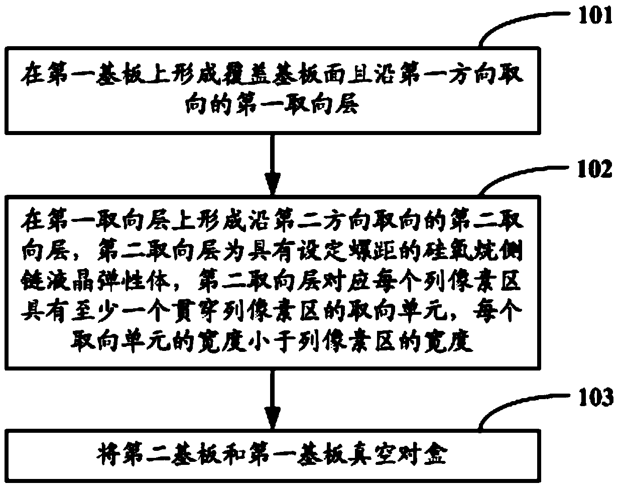
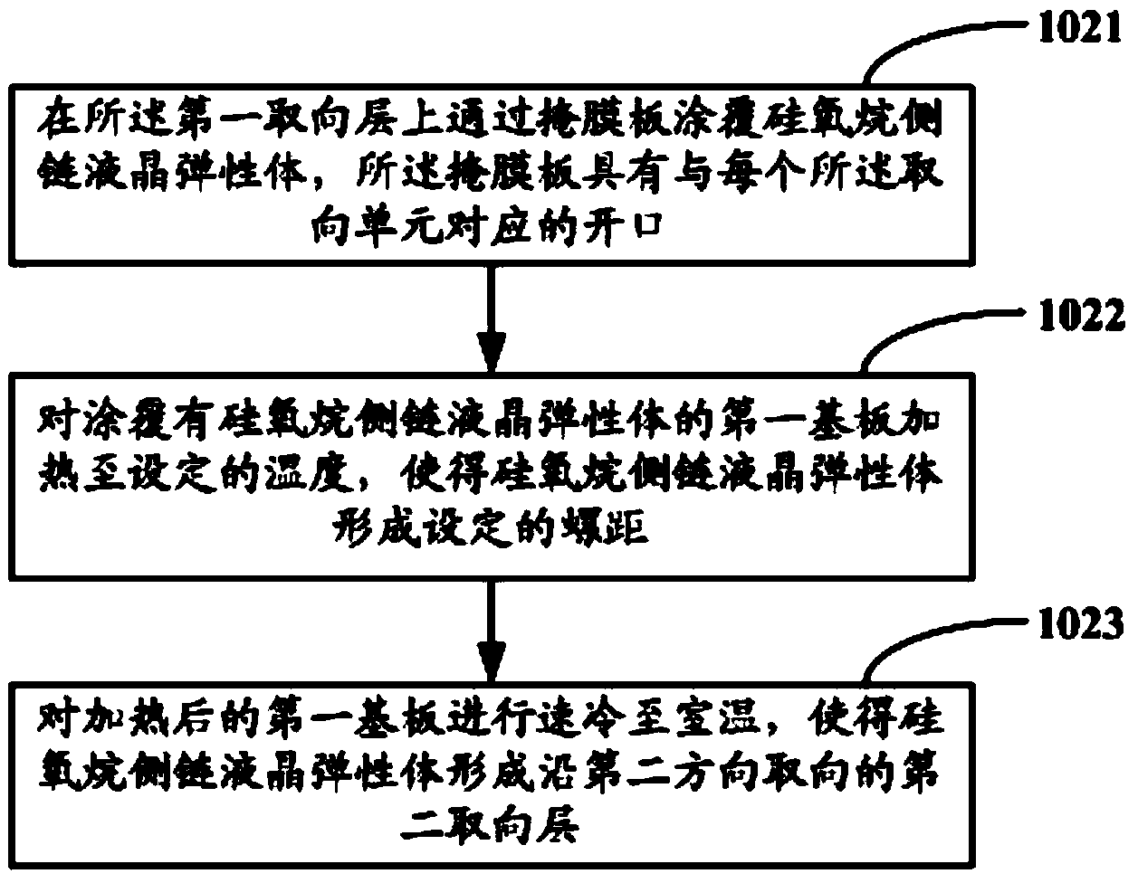
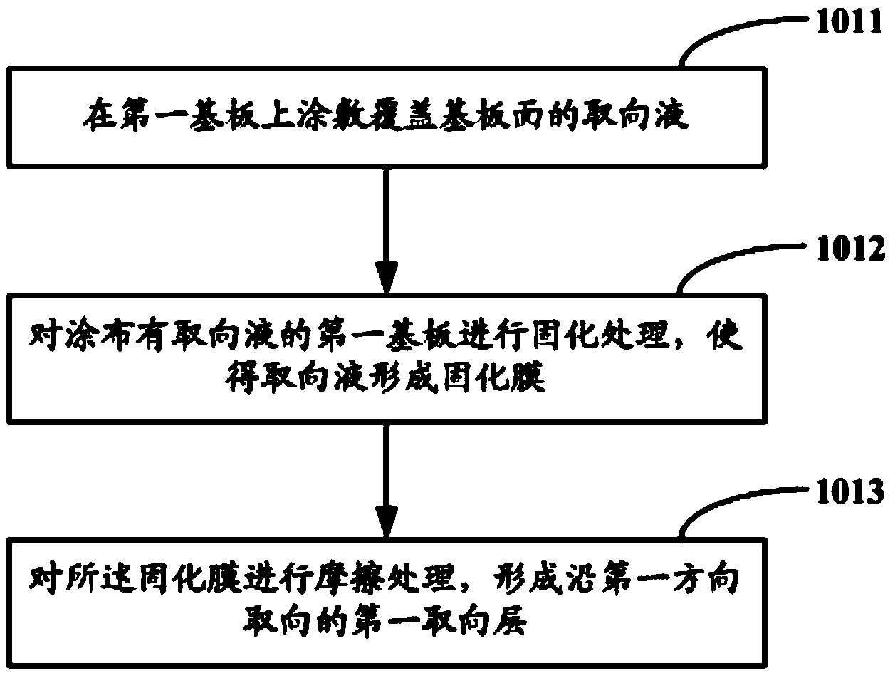
The invention relates to the field of the liquid crystal display technology and discloses a liquid crystal display panel, a display device and a method for manufacturing the liquid crystal display panel. The method for manufacturing the liquid crystal display panel comprises the steps that a first orientation layer is formed on a first substrate, wherein the surface of the first substrate is covered with the first orientation layer, and orientation is conducted on the first orientation layer in the first direction; a second orientation layer is formed on the first orientation layer, wherein orientation is conducted on the second orientation layer in the second direction, the second orientation layer is an elastic siloxane side chain liquid crystal body with a set screw pitch and is provided with at least one orientation unit which corresponds to each line pixel area and penetrates through the line pixel area, and each orientation unit is narrower than the corresponding line pixel area; a second substrate and the first substrate are combined in a vacuum mode. By the adoption of the method for manufacturing the liquid crystal display panel, it is not needed to conduct friction multiple times in each pixel area, multi-domain display can be achieved simply by manufacturing two orientation layers with different orientation directions, and the manufacturing technology is simplified greatly.

Description

technical field [0001] The invention relates to the technical field of liquid crystal display, in particular to a liquid crystal panel, a display device and a method for manufacturing the liquid crystal panel. Background technique [0002] Among flat panel display devices, Thin Film Transistor Liquid Crystal Display (TFT-LCD for short) has the characteristics of small size, low power consumption, relatively low manufacturing cost and no radiation, and occupies a dominant position in the current flat panel display market. leading position. Common liquid crystal displays can be used as mobile phone display screens, Note Book display screens, GPS display screens, LCD TV display screens, etc. With the advancement of science and technology, the traditional monodomain liquid crystal display has been unable to meet people's requirements for liquid crystal display due to its shortcomings such as low contrast, asymmetric viewing angle, and color shift when viewed from different angl...

Claims


Application Information

Patent Timeline
Patent Type & Authority Applications(China)
IPC IPC(8): G02F1/1337G02F1/1333
Inventor 武晓娟车春城
Owner BOE TECH GRP CO LTD
Learn More