Electromagnetic induction plate structure and manufacturing method thereof, and electromagnetic handwriting input device
A technology of electromagnetic induction and production method, which is applied in the input/output process of data processing, electrical digital data processing, instruments, etc., can solve the problems such as the inability to meet the thinning of products and the inability to effectively reduce the overall thickness of the digital board, so as to reduce the overall The effect of thickness
- Summary
- Abstract
- Description
- Claims
- Application Information
AI Technical Summary
Problems solved by technology
Method used
Image

Examples
no. 1 example 〕
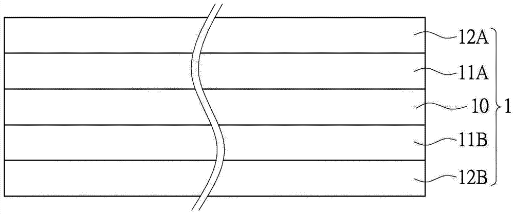
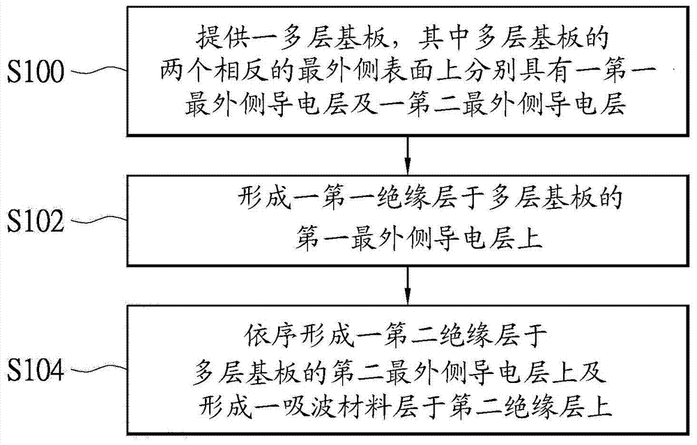
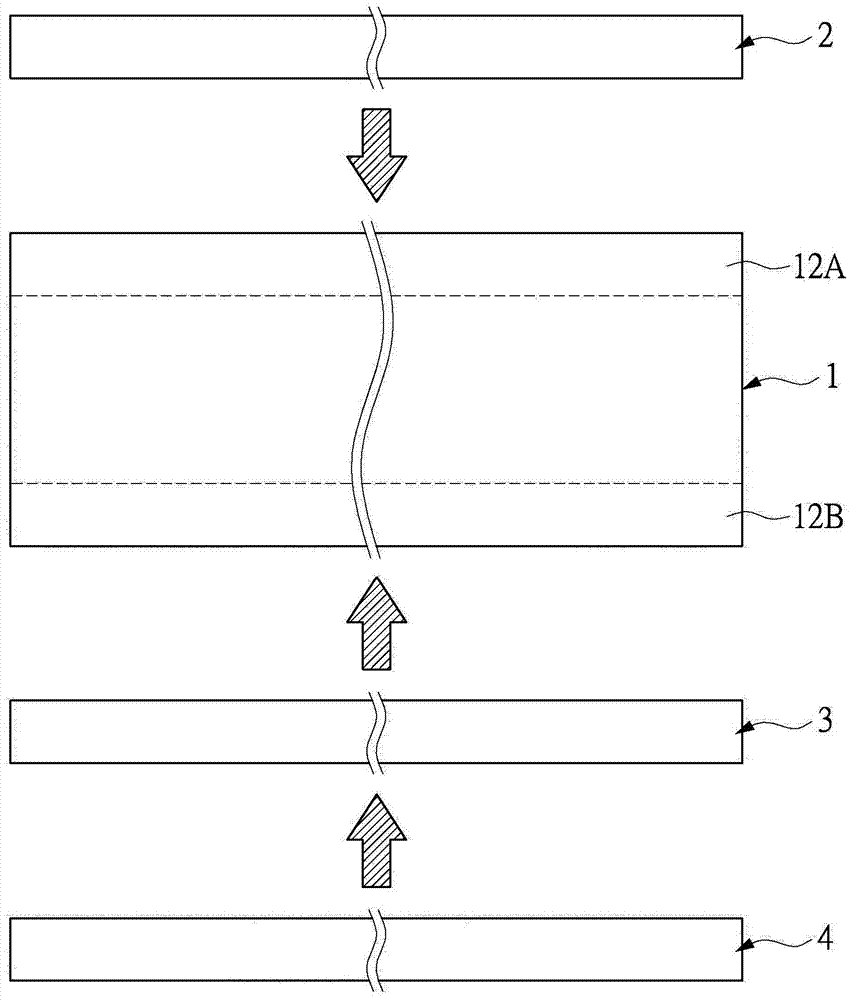
[0053] see figure 1 ,and Figure 2A to Figure 2C As shown, the first embodiment of the present invention provides a manufacturing method of the electromagnetic induction plate structure M (or antenna plate structure), which may include the following steps: first, as figure 1 As shown, a multilayer substrate 1 is provided, wherein two opposite outermost surfaces of the multilayer substrate 1 respectively have a first outermost conductive layer 12A and a second outermost conductive layer 12B (S100); then, Cooperate Figure 2B and Figure 2C As shown, a first insulating layer 2 is formed on the first outermost conductive layer 12A of the multilayer substrate 1 by coating, printing or any other forming method (as shown by the solid arrow) (S102), so that The first insulating layer 2 may directly contact the first outermost conductive layer 12A of the multilayer substrate 1; then, cooperate Figure 2B and Figure 2CAs shown, a second insulating layer 3 is sequentially formed o...
no. 2 example
[0060] see figure 1 ,and Figure 3A to Figure 3C As shown, the second embodiment of the present invention provides a method for manufacturing an electromagnetic induction panel structure M, which may include the following steps: first, as figure 1 As shown, a multilayer substrate 1 is provided, wherein two opposite outermost surfaces of the multilayer substrate 1 respectively have a first outermost conductive layer 12A and a second outermost conductive layer 12B (S200); then, Cooperate Figure 3B and Figure 3C As shown, a first insulating layer 2 is attached (as shown by a hollow arrow) on the first outermost conductive layer 12A of the multilayer substrate 1 through a first adhesive layer 6 (S202), so that the first adhesive Layer 6 is disposed between the first insulating layer 2 and the first outermost conductive layer 12A of the multilayer substrate 1; Figure 3B and Figure 3C As shown, a second insulating layer 3 is sequentially formed on the second outermost condu...
no. 3 example
[0063] see figure 1 ,and Figure 4A to Figure 4C As shown, the third embodiment of the present invention provides a method for manufacturing an electromagnetic induction plate structure M, which may include the following steps: first, as figure 1 As shown, a multilayer substrate 1 is provided, wherein two opposite outermost surfaces of the multilayer substrate 1 respectively have a first outermost conductive layer 12A and a second outermost conductive layer 12B (S300); then, Cooperate Figure 4B and Figure 4C As shown, a first insulating layer 2 is formed on the first outermost conductive layer 12A of the multilayer substrate 1 by coating, printing or any other forming method (as shown by the solid arrow) (S302), so that The first insulating layer 2 may directly contact the first outermost conductive layer 12A of the multilayer substrate 1; then, cooperate Figure 4B and Figure 4C As shown, a prefabricated three-layer structure formed by sequentially stacking a second a...
PUM
| Property | Measurement | Unit |
|---|---|---|
| thickness | aaaaa | aaaaa |
| thickness | aaaaa | aaaaa |
Abstract
Description
Claims
Application Information
 - R&D
- Intellectual Property
- Life Sciences
- Materials
- Tech Scout
- Unparalleled Data Quality
- Higher Quality Content
- 60% Fewer Hallucinations
Browse by: Latest US Patents, China's latest patents, Technical Efficacy Thesaurus, Application Domain, Technology Topic, Popular Technical Reports.
© 2025 PatSnap. All rights reserved.Legal|Privacy policy|Modern Slavery Act Transparency Statement|Sitemap|About US| Contact US: help@patsnap.com