

Conductive element and method of manufacture thereof, wiring element, and master
A technology for conductive elements and master disks, applied in the field of master disks, can solve the problems of easy blockage of mask holes, expensive screen printing masks, difficulty in accurately positioning masks, etc., and achieves the effect of high production capacity and excellent optical characteristics.
Inactive Publication Date: 2014-12-03
SONY CORP
View PDF0 Cites 1 Cited by
- Summary
- Abstract
- Description
- Claims
- Application Information
AI Technical Summary
Problems solved by technology
[0004] However, the problem with screen printing is that the mask is expensive, it is difficult to position the mask accurately, and the holes of the mask are easy to clog
Method used
View moreImage
Smart ImageViewing Examples

Examples
no. 7 approach
[0096] 7. Seventh Embodiment (Example of Conductive Element Using an Impenetrable Substrate)
no. 8 approach
[0097] 8. Eighth Embodiment (Example of Transfer Device Using Steps to Transport a Substrate)
no. 9 approach
[0098] 9. Ninth Embodiment (Example of Transfer Device Provided with an Endless Belt Master)
[0099] 10. Tenth Embodiment (Example of Forming Conductive Pattern Sections on Both Surfaces of a Substrate)
[0100] 11. Eleventh embodiment (example using a plurality of impermeable structures)
[0101] 12. Twelfth embodiment (example of forming a concave structure)
Login to View More PUM
| Property | Measurement | Unit |
|---|---|---|
| thickness | aaaaa | aaaaa |
| thickness | aaaaa | aaaaa |
Abstract
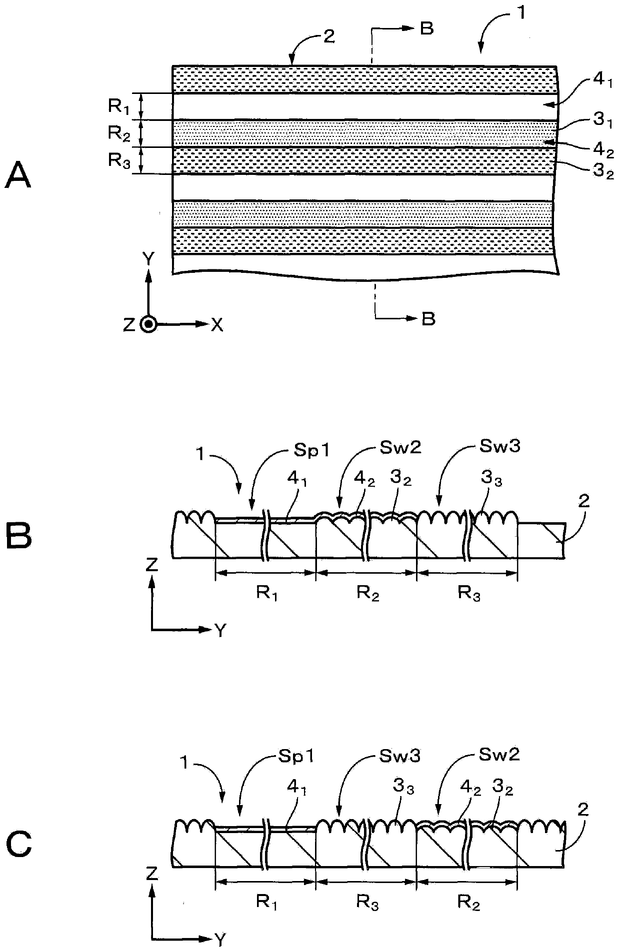
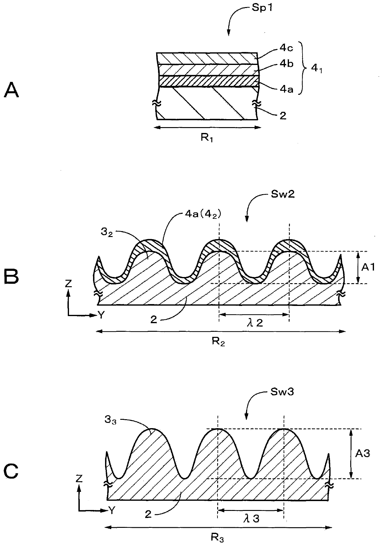
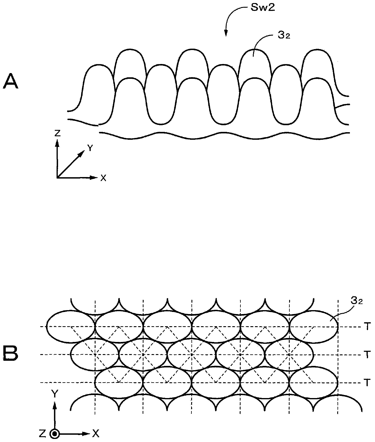
A conductive element comprises: a base having a first wave surface, a second wave surface and a third wave surface; a first layer provided on the first wave surface; and a second layer formed on the second wave surface. The first layer has a laminated structure obtained by laminating two or more layers; the second layer has a single-layer structure or laminated structure comprising some of the layer(s) of the first layer; the first layer and the second layer form a conductive pattern section. The first wave surface, the second wave surface and the third wave surface satisfy the relationship: 0 <=(Am1 / lambdam1)<(Am2 / lambdam2)<(Am3 / lambdam3) <= 1.8 (where Am1 is the average amplitude of oscillation of the first wave surface, Am2 is the average amplitude of oscillation of the second wave surface, Am3 is the average amplitude of oscillation of the third wave surface, lambdam1 is the average wavelength of the first wave surface, lambdam2 is the average wavelength of the second wave surface, and lambdam3 is the average wavelength of the third wave surface).
Description
technical field [0001] The technology relates to a conductive element, a method for manufacturing the conductive element, a wiring element, and a master. Specifically, the present technology relates to a conductive element having a conductive pattern portion formed on a surface of a substrate. Background technique [0002] Hitherto, as a method of forming a conductive layer having a predetermined circuit pattern on an insulating substrate made of glass, plastic, or the like, a method of forming a circuit pattern using a photolithographic technique has been widely used. In a method of forming a circuit pattern, a step-and-repeat method or the like is generally used. Specifically, in the forming method, through the processes of "metal layer coating", "resist coating", "exposure", "development", "removal" and "resist stripping" performed in this order to form circuit pattern. Therefore, the method of forming circuit patterns using the photolithographic technique has low thro...
Claims
Login to View More Application Information
Patent Timeline
 Patent Type & Authority Applications(China)
IPC IPC(8): H01B5/14G06F3/041G09F9/00H05B33/14H05K3/10
CPCH05K3/0014H05B33/14G06F3/041H05K3/06H05K3/389H05K2203/0143G09F9/00H05K2201/0326H05K2203/0108H05K2201/0317H05K2203/0537H05K1/02H05K1/0306H05K3/02H05K2201/09027H05K2203/10
Inventor 林部和弥田泽洋志梶谷俊一
Owner SONY CORP