Chip pin exchanging method for circuit diagram design

A circuit diagram design, pin technology, applied in computing, electrical digital data processing, special data processing applications, etc., can solve the problems of inability to guarantee correctness, low PCB routing rate, rising cost, etc., to achieve convenient and fast PCB routing, Improve the efficiency of generation and ensure the effect of correctness

Inactive Publication Date: 2014-12-10
SHENZHEN FASTPRINT CIRCUIT TECH +2
View PDF2 Cites 8 Cited by
  • Summary
  • Abstract
  • Description
  • Claims
  • Application Information

AI Technical Summary

Problems solved by technology

At present, the design process generally adopts the design of the circuit schematic diagram first, and then imports it into the PCB design. However, the pin swap requirement is proposed after consideration of comprehensive factors such as layout, wiring, and signal flow during the PCB design process, and needs to be submitted for changes. Reporting to the schematic diagram side, the traditional method is to manually analyze which pins need to be swapped one by one, and then write a report. When the number of chip pins that need to be swapped reaches hundreds or even thousands, it is difficult to complete the swap logic manually , and the correctness cannot be guaranteed
[0003] For example, the number of pins of Xilinx Virtex-6 FPGA chip reaches 1156, and the signal connection direction is irregular. If the current signal connection relationship is not carried out, the PCB layout rate is very low; and it is necessary to increase the corresponding layer to ensure the layout rate. , leading to an increase in cost

Method used


Image

  • Chip pin exchanging method for circuit diagram design
  • Chip pin exchanging method for circuit diagram design
  • Chip pin exchanging method for circuit diagram design

Examples


Embodiment Construction

[0022] It should be noted that, in the case of no conflict, the embodiments in the present application and the features in the embodiments can be combined with each other.

[0023] A circuit diagram design chip pin exchange method, which comprises steps:

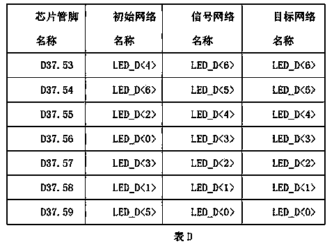
[0024] S10, for the pins that need to be exchanged in the chip 1, go out according to the optimal way, and generate a relationship list A of the pin names and the corresponding initial network names in the first order. For pin 2 that can be exchanged in chip 1, it is routed according to the optimal outlet method, without considering the signal flow direction, so that the wiring channels of the chip can be fully utilized. Usually, the best way to go out is just to pull out the pin signal to the periphery of chip 1 (such as figure 1 shown). Of course, the optimal wiring method is different according to the specific circuit wiring situation. For example, sometimes it is necessary to lead the pin 2 of the chip to different lev...


PUM


Abstract

The invention discloses a chip pin exchanging method for circuit diagram design. The chip pin exchanging method comprises the following steps: S10, conducting wire outgoing according to an optimal wire outgoing method for pins needed to be exchanged, and generating a relation list A of pin names and corresponding initial network names according to a first sequence; S20, distributing external signals needed to be connected to a chip for pin exchange to the positions close to the wire outgoing position of the chip, forming a sequence-identified corresponding relation area through pin outgoing wires and the signals, and generating a signal network name list B corresponding to the signals according to a first sequence; S30, changing the initial network names corresponding to the chip pin ends in a schematic diagram into target network names according to the contents of the list A and the list B so as to make the changed target network names correspond to the list B when arranging the target network names according to the first sequence. The chip pin exchanging method for circuit diagram design effectively improves routability of PCB wiring, greatly increases pin exchange list generating efficiency, and effectively ensures exchange correctness of the pins. The chip pin exchanging method can be widely applied to circuit diagram design.

Description

technical field [0001] The invention relates to the field of circuit diagram design, in particular to a circuit diagram pin exchange method. Background technique [0002] With the development of science and technology, the number of chip pins and the design density are increasing day by day in electronic circuit design, and the difficulty of electronic circuit design is becoming more and more difficult. Most electronic circuit designs require pin network exchange for certain chips to adapt to Physical space requirements for circuit design. At present, the design process generally adopts the design of the circuit schematic diagram first, and then imports it into the PCB design. However, the pin swap requirement is proposed after consideration of comprehensive factors such as layout, wiring, and signal flow during the PCB design process, and needs to be submitted for changes. Reporting to the schematic diagram side, the traditional method is to manually analyze which pins nee...

Claims


Application Information

Patent Timeline
Patent Type & Authority Applications(China)
IPC IPC(8): G06F17/50
Inventor 郭东胜蒋学东
Owner SHENZHEN FASTPRINT CIRCUIT TECH
Why Eureka
Try Eureka