Eureka AIR delivers breakthrough ideas for toughest innovation challenges, trusted by R&D personnel around the world.

Welding pad structure and display device

A display device and welding pad technology, which is applied to static indicators, instruments, electrical components, etc., can solve problems such as poor flatness of the welding pad structure, influence on signal transmission, abnormal ACF, etc., and achieve the effect of improving uneven contact resistance

Active Publication Date: 2014-12-10
BOE TECH GRP CO LTD +1
View PDF5 Cites 2 Cited by
  • Summary
  • Abstract
  • Description
  • Claims
  • Application Information

AI Technical Summary

Problems solved by technology

[0005] Based on some problems existing in the current COG process, such as in the above-mentioned COG structure, the flatness of the pad structure is not good, the ACF is abnormal, and the two pads that are electrically connected have alignment offsets, etc., which will cause the pad structure to be damaged. The contact resistance of different welding areas is uneven, which affects the transmission of signals, resulting in the hidden danger of abnormal display in the subsequent use of display products, and the contact resistance of the pad structure will also change with the accumulation of time, temperature and humidity
[0006] Therefore, how to improve the defective display products caused by the non-uniform contact resistance of different welding areas of the pad structure is a technical problem that those skilled in the art need to solve urgently.

Method used


Image

  • Welding pad structure and display device
  • Welding pad structure and display device
  • Welding pad structure and display device

Examples


Embodiment Construction

[0039] The specific implementation manners of the pad structure and the display device provided by the embodiments of the present invention will be described in detail below with reference to the accompanying drawings.

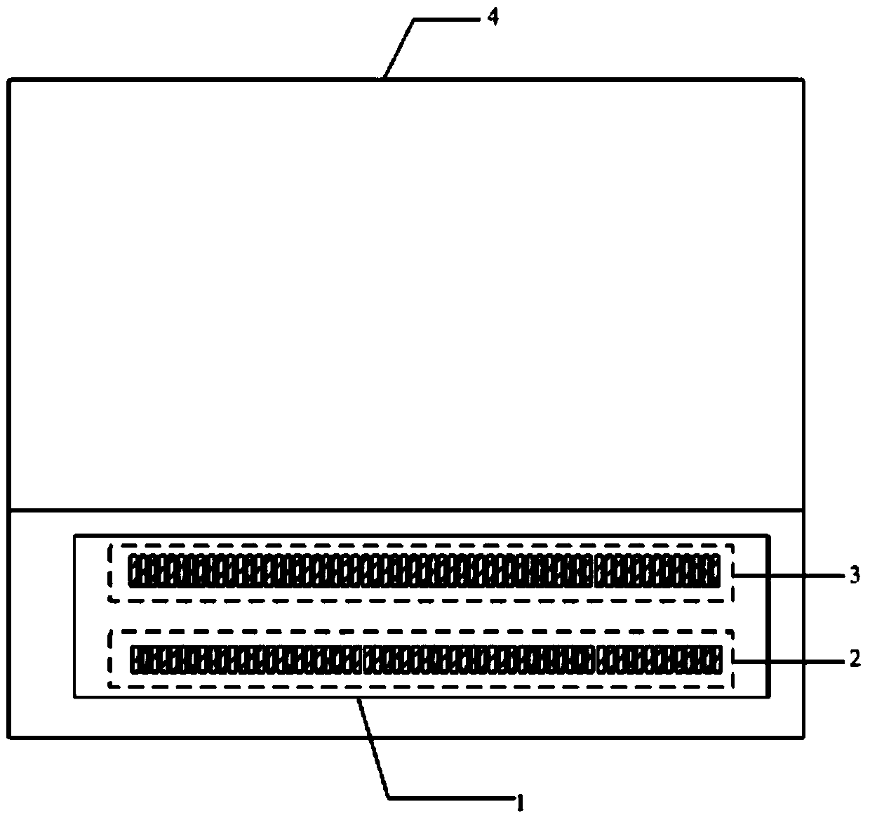
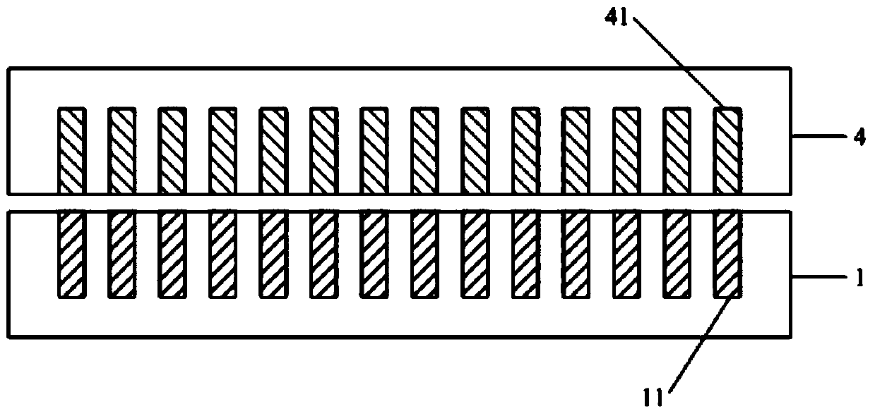
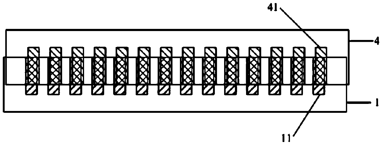
[0040] A pad structure provided by an embodiment of the present invention, such as image 3 As shown, it includes a first welding pad unit 100 and a second welding pad unit 200 that are electrically connected by crimping, wherein the first welding pad unit 100 has a plurality of first welding pads 101 arranged side by side, and the second welding pad unit 100 has a plurality of first welding pads 101 arranged side by side. The pad unit has a plurality of second welding pads 201 arranged side by side, and each second welding pad 201 is electrically connected to the corresponding first welding pad 101; the first welding pad unit 100 is divided into at least two welding areas ( image 3 The area surrounded by each dotted line box in the above is a welding area), an...


PUM


Abstract

The invention discloses a welding pad structure and a display device. The welding pad structure comprises a first welding pad unit and a second welding pad unit which are electrically connected by crimping; the first welding pas unit is divided into at least two welding areas, namely the welding pad structure is divided into at least two welding areas, and a detection unit is arranged for each welding area, so that contact resistance between a first welding pad plate and a second welding pad plate in each welding area can be estimated by a detection welding pad plate and a comparison circuit in the corresponding detection unit, and thereby current of different welding areas can be adjusted according to estimated result, and influence on signal transmission caused by nonuniform contact resistance of different welding areas of the welding pad structure can be improved; and therefore, when the welding pad structure is applied to a display device, the problem that the display product is unqualified due to nonuniform contact resistance of different welding areas of the welding pad structure can be overcome.

Description

technical field [0001] The invention relates to the technical field of semiconductors, in particular to a pad structure and a display device. Background technique [0002] With the development of the electronics and communication industries, the development of light-emitting diodes (Light Emitting Diode, LED), organic light-emitting diodes (Organic Light Emitting Diode, OLED), plasma displays (Plasma Display Panel, PDP) and liquid crystal displays (Liquid Crystal Display, LCD) ) and other flat panel display devices are increasing day by day. The development trend of flat panel display devices is light, thin, short, and small. Packaging technology with high density, small volume, and high installation freedom is required to meet the above requirements. Therefore, Chip on Glass (COG) packaging Technology came into being. [0003] COG is to fix the driver chip on the display panel, use the display panel as the carrier for packaging the driver chip, and bond the driver chip wi...

Claims


Application Information

Patent Timeline
IPC IPC(8): H01L23/488G09G3/00
Inventor 张郑欣朱红徐帅
Owner BOE TECH GRP CO LTD
Why Eureka
Eureka Blog
Learn More