

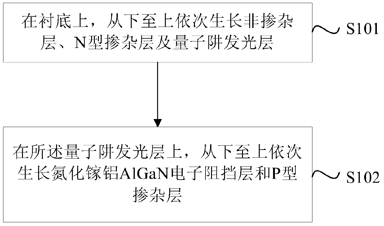
Light emitting diode epitaxy and growing method of light emitting diode electronic barrier layer
An electron blocking layer and light-emitting diode technology, which is applied in circuits, electrical components, semiconductor devices, etc., can solve the problems of poor crystal quality and lattice mismatch, and achieve the effect of reducing the degree of lattice mismatch and improving the recombination efficiency.
- Summary
- Abstract
- Description
- Claims
- Application Information
AI Technical Summary
Problems solved by technology
Method used
Image

Examples
Embodiment 1
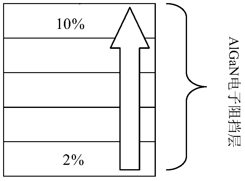
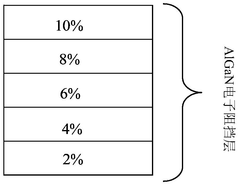
[0038] The 60nm AlGaN electron blocking layer of light-emitting diodes was grown by the gradual gradient change doping method, [Al x GaN 1-x (2%
[0039] 1) Sapphire (Al 2 o 3 ) The patterned substrate is placed in the reaction chamber, and the flow rate is 110L / min of H 2 Heating to 1100°C and baking for 7 minutes under the atmosphere, the pressure of the reaction chamber is 500Torr;
[0040] 2) Grow a GaN buffer layer with a thickness of 40nm at 540°C, where the reaction chamber pressure is 500Torr, N 2 、H 2 and NH 3 The flow ratio is 75:150:56;
[0041] 3) Grow a GaN undoped layer with a thickness of 2000nm at 1070°C, wherein the reaction chamber pressure is 200Torr, N 2 、H 2 and NH 3 The flow ratio is 75:150:56;
[0042] 4) Grow a silicon-doped N-type GaN doped layer with a thickness of 1400 nm at 1080° C., wherein the reaction chamber pressure is 200 Torr, N 2 、H 2 and NH 3 The flow ratio is 64:120:50;
[0043] 5) Grow a GaN / InGaN / GaN quantum well l...
Embodiment 2
[0048] The 45nm AlGaN electron blocking layer of light-emitting diodes was grown by the transition gradient change doping method, [Al x GaN 1-x (2%
[0049] 1) Sapphire (Al 2 o 3 ) The patterned substrate is placed in the reaction chamber, and the flow rate is 110L / min of H 2 Heating to 1100°C and baking for 7 minutes under the atmosphere, the pressure of the reaction chamber is 500Torr;
[0050] 2) Grow a GaN buffer layer with a thickness of 40nm at 540°C, where the reaction chamber pressure is 500Torr, N 2 、H 2 and NH 3 The flow ratio is 75:150:56;
[0051] 3) Grow a GaN undoped layer with a thickness of 2500nm at 1070°C, wherein the reaction chamber pressure is 200Torr, N 2 、H 2 and NH 3 The flow ratio is 75:150:56;
[0052] 4) Grow a silicon-doped N-type GaN doped layer with a thickness of 1400 nm at 1080° C., wherein the reaction chamber pressure is 200 Torr, N 2 、...
Embodiment 3
[0058] The 42nm AlGaN electron blocking layer of light-emitting diodes was grown by the transition gradient change doping method, [Al x GaN 1-x (3%
[0059] 1) Sapphire (Al 2 o 3 ) The patterned substrate is placed in the reaction chamber, and the flow rate is 110L / min of H 2 Heating to 1100°C and baking for 7 minutes under the atmosphere, the pressure of the reaction chamber is 500Torr;
[0060] 2) Grow a GaN buffer layer with a thickness of 40nm at 540°C, where the reaction chamber pressure is 500Torr, N 2 、H 2 and NH 3 The flow ratio is 75:150:56;
[0061] 3) Grow a GaN undoped layer with a thickness of 2500nm at 1070°C, wherein the reaction chamber pressure is 200Torr, N 2 、H 2 and NH 3 The flow ratio is 75:150:56;
[0062] 4) Grow a silicon-doped N-type GaN doped layer with a thickness of 1400 nm at 1080° C., wherein the reaction chamber pressure is 200 Torr, N 2 、H 2...
PUM
 Abstract
Description
Claims
Application Information