Pixel circuit, organic electroluminescent display panel and display device
A pixel circuit and light-emitting device technology, applied in static indicators, instruments, etc., can solve problems such as uneven brightness of images, and achieve the effect of improving uniformity
- Summary
- Abstract
- Description
- Claims
- Application Information
AI Technical Summary
Problems solved by technology
Method used
Image
Examples
example 1
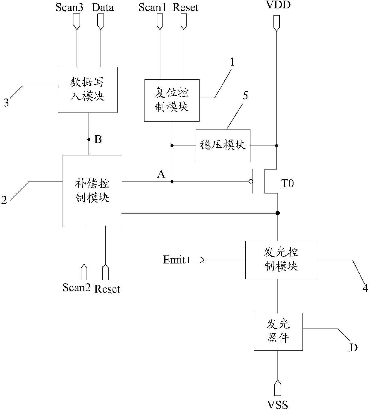
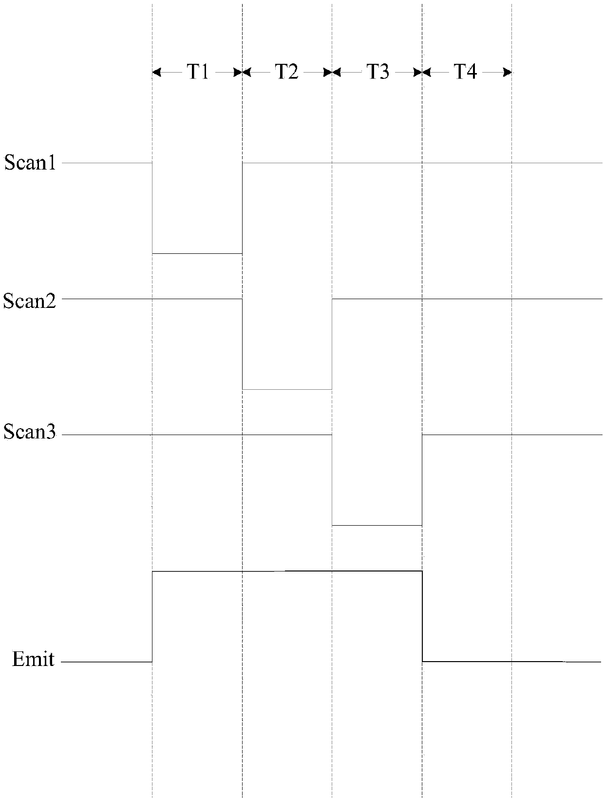
[0090] by Figure 4a The structure of the pixel circuit shown is taken as an example to describe its working process, in which Figure 4a In the pixel circuit shown, the driving transistor is a P-type transistor, and all switching transistors are P-type transistors. Each P-type transistor is turned off under the action of a high level and turned on under the action of a low level; the corresponding input timing diagram is as follows Figure 3a shown. Specifically, choose the Figure 3a The four stages T1, T2, T3 and T4 in the input timing diagram shown.
[0091] In the T1 stage, Scan1=0, Scan2=1, Scan3=1, Emit=1. The second switch transistor T2 , the third switch transistor T3 , the fourth switch transistor T4 and the fifth switch transistor T5 are all in an off state, and the first switch transistor T1 is in an on state. The reset signal Reset is transmitted to the first node A through the turned-on first switching transistor T1, so that the driving transistor T0 is turne...
example 2
[0096] by Figure 4b The structure of the pixel circuit shown is taken as an example to describe its working process, in which Figure 4b In the pixel circuit shown, the driving transistor is a P-type transistor, and all switching transistors are N-type transistors. Each N-type transistor is turned off under the action of a low level and turned on under the action of a high level; the corresponding input timing diagram is as follows Figure 3b shown. Specifically, choose the Figure 3b The four stages T1, T2, T3 and T4 in the input timing diagram shown.
[0097] In the T1 stage, Scan1=1, Scan2=0, Scan3=0, Emit=0. The second switch transistor T2 , the third switch transistor T3 , the fourth switch transistor T4 and the fifth switch transistor T5 are all in an off state, and the first switch transistor T1 is in an on state. The reset signal Reset is transmitted to the first node A through the turned-on first switching transistor T1, so that the driving transistor T0 is turne...
PUM
 Abstract
Description
Claims
Application Information


