
Magnetic tunnel junction unit and spinning electronic device

A technology of spintronic devices and magnetic tunnel junctions, applied in the direction of electric solid devices, electrical components, semiconductor devices, etc., can solve the problems of not making full use of the flipping effect, not being able to fully reduce the flipping current density, not making full use of the weakening effect, etc. Achieve the effects of increasing the degree of magnetization switching, reducing the current density of magnetization switching, and increasing the TMR value

Active Publication Date: 2014-12-17
HUAZHONG UNIV OF SCI & TECH
View PDF5 Cites 6 Cited by
  • Summary
  • Abstract
  • Description
  • Claims
  • Application Information

AI Technical Summary

Problems solved by technology

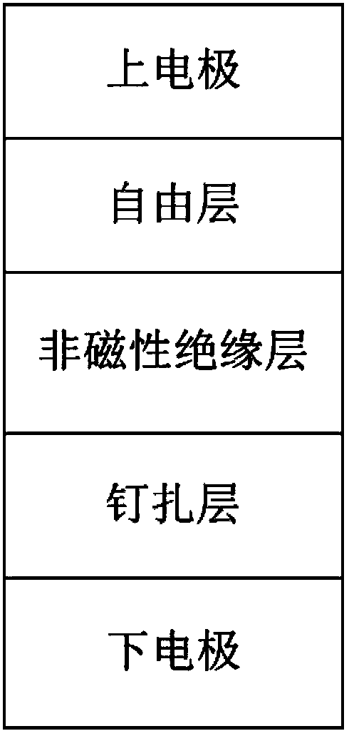
[0008] Aiming at the improvement requirements of the prior art, the present invention provides a magnetic tunnel junction unit, the purpose of which is to effectively reduce the magnetization switching current density and improve the degree of magnetization switching of the free layer, thereby solving the problem that the existing magnetic tunnel junction unit has no Make full use of the flipping effect of spin electrons on the magnetic moment of the free layer, and do not make full use of the weakening effect of Joule heat on the magnetic anisotropy strength during the flipping process of the free layer, resulting in the inability to sufficiently reduce the flipping current density and improve the TMR of the MTJ memory cell value technical issues

Method used


Image

  • Magnetic tunnel junction unit and spinning electronic device
  • Magnetic tunnel junction unit and spinning electronic device
  • Magnetic tunnel junction unit and spinning electronic device

Examples


Embodiment Construction

[0029] In order to make the object, technical solution and advantages of the present invention more clear, the present invention will be further described in detail below in conjunction with the accompanying drawings and embodiments. It should be understood that the specific embodiments described here are only used to explain the present invention, not to limit the present invention. In addition, the technical features involved in the various embodiments of the present invention described below can be combined with each other as long as they do not constitute a conflict with each other.

[0030] The magnetic tunnel junction unit provided by the embodiment of the present invention can be applied in a magnetic random access memory, and the magnetic random access memory includes a plurality of magnetic tunnel junction memory cells arranged in an array, and the magnetic tunnel junction memory cell can effectively improve the TMR of the STT-MRAM device value, and reduce its free la...


PUM


Abstract

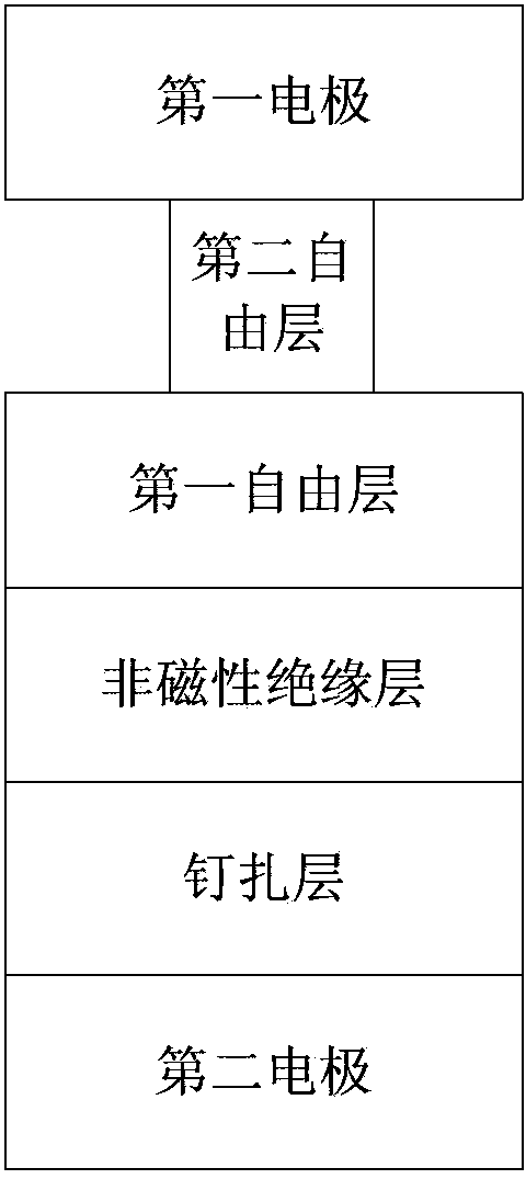
The invention discloses a tunnel junction unit and a magnetoresistive random access memory. The tunnel junction unit comprises a first electrode, a first free layer, a non-magnetic insulating layer, a pinning layer and a second electrode which are connected in sequence, and further comprises a second free layer connected between the first electrode and the first free layer, wherein the cross sectional area of the second free layer is smaller than the cross sectional area of the free layer; the second free layer and the first free layer form a composite free layer structure together; the second free layer is used for gathering current in order that the current density on the second free layer is higher than the current density on the first free layer, so that the magnetic torque of the second free layer is overturned before the first free layer; and overturning of the magnetic torque of the first free layer is driven by overturning of the second free layer under an exchange coupling interaction between the second free layer and the first free layer. Through adoption of the tunnel junction unit and the magnetoresistive random access memory, the magnetic overturning degree of the composite free layer in a magnetic tunnel junction unit is increased, the overturning current density of the composite free layer is lowered, and the TMR (Tunnel Magnetic Resistance) value of the magnetic tunnel junction unit is increased under the same current density excitation condition.

Description

technical field [0001] The invention belongs to the field of spin electronic devices, and more specifically relates to a tunnel junction unit and a magnetic random access memory. Background technique [0002] The rapid popularization of computer networks around the world makes the amount of data that people need to store, process and transmit grow exponentially, and the huge amount of data puts forward new requirements for storage technology. As one of the main information storage technologies, solid-state memory is mainly used in computer main memory and storage chips of various portable electronic products. In recent years, its market growth rate is much higher than that of other storage devices such as hard drives. , fast read and write speed, low power consumption, and low noise solid-state hard drives are sought after, and solid-state memory will have a broader market prospect. [0003] The solid-state memory chips currently used for computer main memory are mainly dyn...

Claims


Application Information

Patent Timeline
Patent Type & Authority Applications(China)
IPC IPC(8): H01L27/10H01L27/115G11C11/16H10B69/00
CPCG11C11/16
Inventor 缪向水倪含程晓敏
Owner HUAZHONG UNIV OF SCI & TECH
Learn More