

Flip chip plastic package structure with cooling structure and manufacturing method
A technology of flip-chip and heat dissipation structure, which is applied in semiconductor/solid-state device manufacturing, semiconductor/solid-state device components, semiconductor devices, etc., can solve the problems of poor heat dissipation and high cost, and achieve good heat dissipation performance, low cost, Good cooling effect
- Summary
- Abstract
- Description
- Claims
- Application Information
AI Technical Summary
Problems solved by technology
Method used
Image

Examples
Embodiment 1
[0027] In order to enable those skilled in the art to understand the present invention in more detail, the present invention will be described in detail below in conjunction with the accompanying drawings.
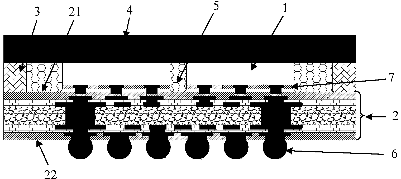
[0028] like figure 1 said, figure 1 It is a flip-chip plastic packaging structure with a heat dissipation structure in an embodiment of the present invention, wherein the structure includes:
[0029] Chip 1;
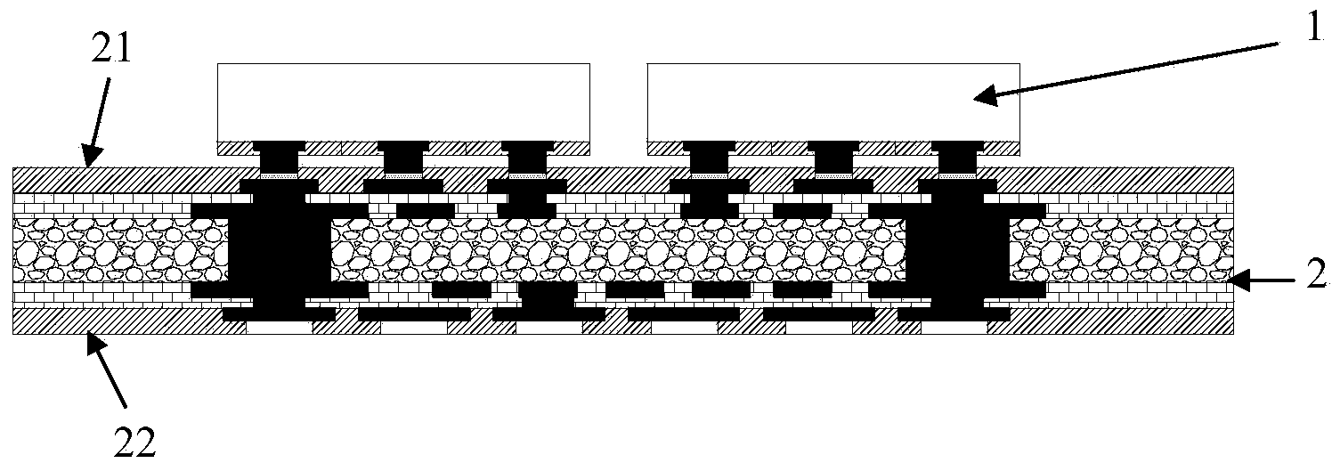
[0030] a substrate 2, the chip 1 is disposed on the first surface 21 of the substrate 2;
[0031] a height limiting block 3, the height limiting block 3 is arranged on the first surface 21 of the substrate 2;
[0032] Specifically, the height-limiting block 3 can be made of metal, plastic, silicon, etc., and the height-limiting block 3 is mainly used to support the heat dissipation plate 4, and the height-limiting block and the chip are set at the same height, thereby ensuring The heat dissipation plate 4 is parallel to the substrate 2 . Further, both the height...
Embodiment 2
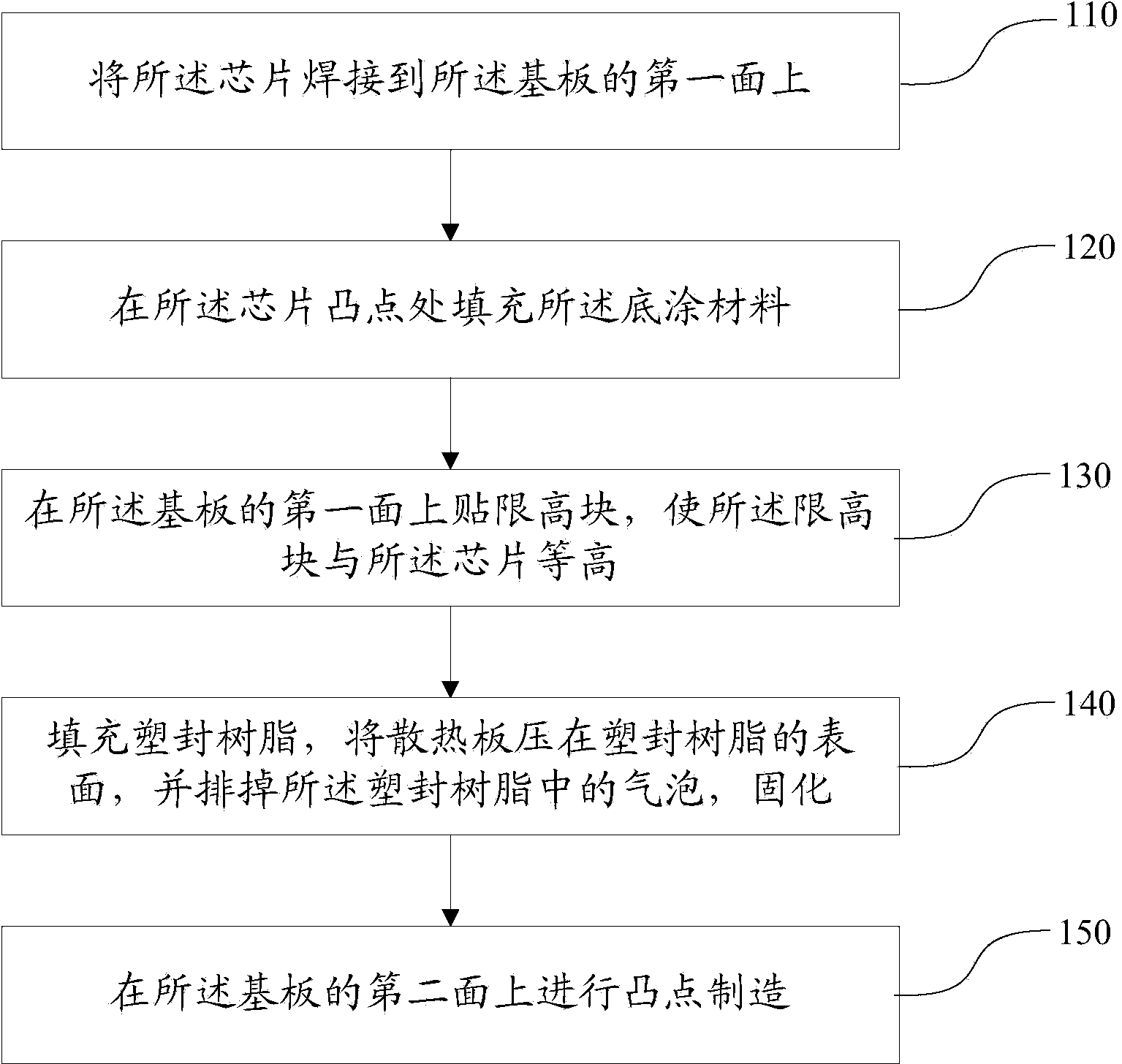
[0045] like Figure 2-7 As shown, the embodiment of the present invention also provides a flip-chip plastic packaging manufacturing method with a heat sink, the method comprising:
[0046] Step 110: welding the chip 1 onto the first surface 21 of the substrate 2;
[0047] Specifically, step 110 may specifically be bonding the chip to the substrate in a flip-chip bonding manner.
[0048] Step 120: filling the primer material 7 at the bumps of the chip 1;
[0049] Step 130: paste a height limiting block 3 on the first surface 21 of the substrate 2, so that the height limiting block 3 is equal to the height of the chip 1;
[0050] Step 140: filling the first surface 21 of the substrate 2 with a molding resin 5, pressing the heat dissipation plate 4 on the surface of the molding resin 5, draining the air bubbles in the resin, and curing;
[0051] Specifically, filling the molding resin 5 is to fill in the first space formed by the first surface 21 of the substrate 2 , the heigh...
PUM
 Abstract
Description
Claims
Application Information