Control method of outer layer deviation of circuit board

A control method and circuit board technology, applied in the fields of printed circuit manufacturing, printed circuit, electrical components, etc., can solve the difficult and fast outer layer alignment ability, not to mention the deviation model analysis, optimized alignment ability, positioning holes Damage and other issues

Active Publication Date: 2018-07-20
GUANGZHOU FASTPRINT CIRCUIT TECH +2
View PDF8 Cites 0 Cited by
  • Summary
  • Abstract
  • Description
  • Claims
  • Application Information

AI Technical Summary

Problems solved by technology

[0004] For the first positioning method, since the positioning hole needs to be positioned with a pin, the positioning hole will be damaged and deformed after drilling the through hole and lowering the board. "Damage and deformation" will be more serious, resulting in poor positioning of subsequent blind holes and outer circuit production, resulting in deviation and scrapping
For the second positioning method, since the inner/outer pad of the blind hole is much smaller than the inner/outer pad of the through hole, affected by the greater hole position accuracy of the CNC drilling equipment, the "positioning hole" drilled by the CNC can guarantee blind positioning. The alignment between the hole and the outer layer pad is good, but it is easy to cause the blind hole to be misaligned with the inner layer pad, and the inner short is scrapped
For the third positioning method, there

Method used


Image

  • Control method of outer layer deviation of circuit board
  • Control method of outer layer deviation of circuit board
  • Control method of outer layer deviation of circuit board

Examples


Embodiment Construction

[0026] Embodiments of the present invention are described in detail below:

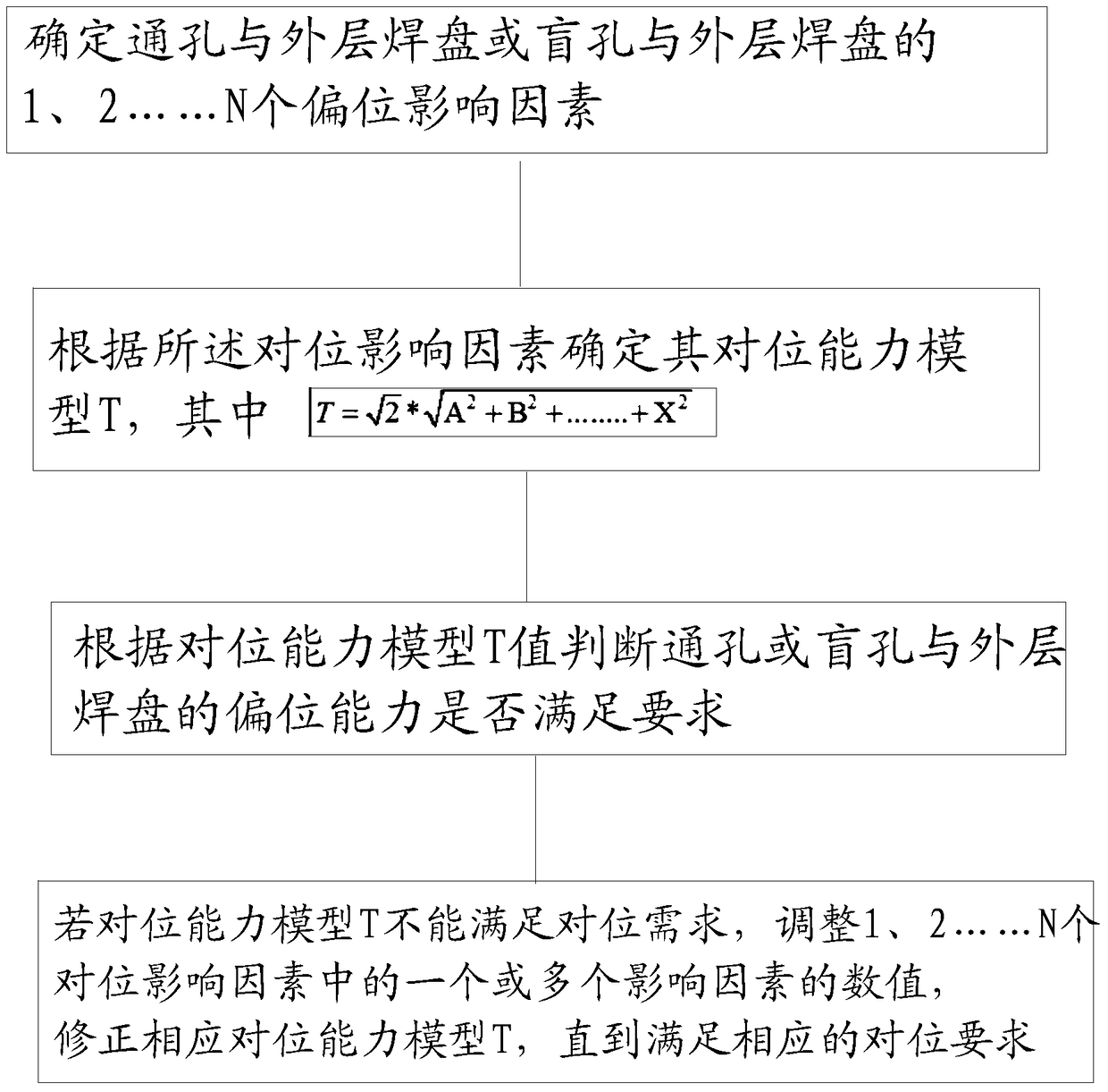
[0027] Determine the 1, 2...N offset influencing factors of through holes or blind holes and outer pads;

[0028] Determine its alignment capability model T according to the offset influencing factors, wherein 1, 2...N offset influence factors correspond to the influence values ​​respectively A, B...X;

[0029] According to the T value of the alignment ability model, judge whether the offset ability of the through hole or blind hole and the outer pad meets the requirements;

[0030] If the alignment ability model T cannot meet the alignment requirements, adjust the values ​​of one or more of the 1, 2...N offset influencing factors, and modify the corresponding alignment ability model T until the corresponding alignment requirements are met. .

[0031] Among them, N represents the unknown specific number of deviation influencing factors, and does not represent its specific number.
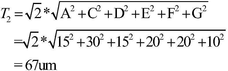
[0032] Taking ...


PUM


Abstract

The invention discloses a control method of outer layer deviation of circuit boards. The control method comprises the steps of determining 1, 2, ..., N deviation influence factors on alignment between a through hole or a blind hole and an outer-layer bonding pad; determining alignment capacity models T according to the deviation influence factors, wherein the influence numerical values corresponding to the 1, 2, ..., N deviation influence factors are A, B, ..., X respectively; judging whether the deviation capacity of the through hole or the blind hole and the bonding pad meets requirements according to the values of the alignment capacity models T; if the alignment capacity models T can not meet the alignment requirements, adjusting the numerical values of one or more of the 1, 2, ..., N deviation influence factors and correcting the corresponding alignment capacity models T till the alignment capacity models T meet the corresponding alignment requirements. By means of the control method, the alignment capacity of different devices in different location modes can be worked out according to the alignment capacity models T, the optimal alignment manufacturing process can be determined by comparison, and therefore production and manufacturing of the circuit boards can be effectively directed.

Description

technical field [0001] The invention relates to the technical field of circuit board production, in particular to a method for controlling the deviation of the outer layer of a circuit board. Background technique [0002] With the development trend of miniaturization, high performance, multi-function and high frequency and high speed of semiconductor products and packaging technology (IC Package), the corresponding packaging substrate must meet the requirements of "miniaturization, ultra-thin, high density", At present, it has excellent and extensive application prospects at home and abroad. Due to the increasingly smaller pitch design of substrate blind holes, this brings great challenges to the alignment control of circuit board manufacturers. Especially the outer layer alignment technology of the substrate (including "blind hole and pad, through hole and pad" offset control), the offset of these outer layers can be directly observed on the appearance of the product, and ...

Claims


Application Information

Patent Timeline
IPC IPC(8): H05K3/00
Inventor 张志强谢添华李志东
Owner GUANGZHOU FASTPRINT CIRCUIT TECH
Why Eureka
Try Eureka