Supercharge Your Innovation With Domain-Expert AI Agents!

Method for packaging semiconductor chip

A chip packaging and semiconductor technology, applied in semiconductor/solid-state device manufacturing, electrical components, circuits, etc., can solve problems affecting packaging quality, low glass transition temperature, high temperature and high pressure resistance, etc., to achieve the effect of improving strength

Active Publication Date: 2015-01-07
HOLYPAO
View PDF8 Cites 0 Cited by
  • Summary
  • Abstract
  • Description
  • Claims
  • Application Information

AI Technical Summary

Problems solved by technology

During the processing of this kind of packaging method, the packaged product needs to withstand high temperature and pressure. If the product to be packaged cannot withstand high temperature and high pressure, this kind of solid material packaging method cannot be used.
Using liquid epoxy encapsulation material at room temperature, injecting it into the mold at low pressure, and using baking to cure can solve the shortcoming of the encapsulated material itself that is not resistant to high temperature and high pressure, but the glass transition temperature (Tg) of liquid epoxy encapsulation material is low , the strength of the cured epoxy packaging material is low, and it is easily affected by high and low temperature mutations (such as reflow soldering, high and low temperature impact, etc.), and abnormal conditions such as surface protrusions and cracks occur, which affect the packaging quality

Method used


Image

  • Method for packaging semiconductor chip
  • Method for packaging semiconductor chip

Examples


Embodiment Construction

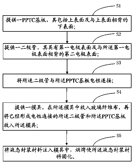
[0025] The present invention will be described in detail below in conjunction with specific embodiments shown in the accompanying drawings. However, these embodiments do not limit the present invention, and any structural, method, or functional changes made by those skilled in the art according to these embodiments are included in the protection scope of the present invention.

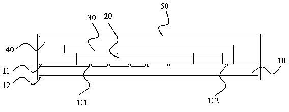
[0026] like figure 1 As shown, in one embodiment of the present invention, the semiconductor chip package structure includes a PPTC substrate 10 , and the PPTC substrate 10 includes an upper surface and a lower surface opposite to the upper surface. The PPTC substrate 10 is composed of multiple single-layer PCT boards. The upper surface of the PPTC substrate 10 is covered with a first insulating layer 11 , and the lower surface of the PPTC substrate 10 is covered with a second insulating layer 12 .

[0027] The diode 20 has a first electrode surface 21 and a second electrode surface 22 opposite to th...


PUM


Abstract

The invention discloses a method for packaging a semiconductor chip. The method comprises the steps that a PPTC substrate is provided and comprises an upper surface and a lower surface opposite to the upper surface; a diode is provided and is provided with a first electrode surface and a second electrode surface opposite to the first electrode surface; the diode is electrically connected with the PPTC substrate; a mold is provided, glass fiber cloth is placed in the mold, and the diode and the PPTC substrate which are connected electrically are placed in the mold; liquid packaging materials are injected into the mold and are baked to be cured. Compared with the prior art, the glass fiber cloth is added into the mold in advance, the packaging structure with glass fibers is obtained after curing, the strength of the packaging materials is obviously improved, and surface protruding, cracking and other abnormal conditions generated by packaging under the circumstance of high and low temperature sudden changes can be avoided well.

Description

technical field [0001] The invention belongs to the field of semiconductor manufacturing, in particular to a semiconductor chip packaging method. Background technique [0002] The traditional semiconductor chip packaging method generally uses high temperature and high pressure to melt the solid packaging material at room temperature and inject it into the mold, and then re-cure quickly (5-50 seconds). During the processing of this packaging method, the packaged product needs to withstand high temperature and pressure. If the product to be packaged cannot withstand high temperature and high pressure, this kind of solid material packaging method cannot be used. Using liquid epoxy encapsulation material at room temperature, injecting it into the mold at low pressure, and using baking to cure can solve the shortcoming of the encapsulated material itself that is not resistant to high temperature and high pressure, but the glass transition temperature (Tg) of liquid epoxy encapsul...

Claims


Application Information

Patent Timeline
IPC IPC(8): H01L21/58H01L21/60
CPCH01L21/565
Inventor 马抗震林昭银李伟沈小英
Owner HOLYPAO
Features
  • R&D
  • Intellectual Property
  • Life Sciences
  • Materials
  • Tech Scout
  • Unparalleled Data Quality
  • Higher Quality Content
  • 60% Fewer Hallucinations
Learn More