Array substrate and display device

A technology of array substrates and substrate substrates, which is applied in the direction of instruments, semiconductor devices, electrical components, etc., can solve the problems of low charging efficiency of pixel electrodes and affect the response speed of flat-panel displays, etc., so as to improve charging efficiency, fast charging, and improve response speed Effect

Inactive Publication Date: 2015-01-07
HEFEI BOE OPTOELECTRONICS TECH +1
View PDF4 Cites 13 Cited by
  • Summary
  • Abstract
  • Description
  • Claims
  • Application Information

AI Technical Summary

Problems solved by technology

[0004] In the existing array substrate, since only part of the drain of the TFT overlaps with the pixel electrode, in this way, when the grayscale signal loaded by the data line passes through the TFT to charge the pixel electrode, it can only charge the pixel electrode from one point on the edge of the pixel electrode. , that is, the position where the pixel electrode is electrically connected to the drain in the TFT starts to charge the pixel electrode, which will lead to low charging efficiency for the pixel electrode, thereby affecting the response speed of the flat panel display

Method used


Image

  • Array substrate and display device
  • Array substrate and display device
  • Array substrate and display device

Examples


Embodiment Construction

[0030] The specific implementation manners of the array substrate and the display device provided by the embodiments of the present invention will be described in detail below with reference to the accompanying drawings.

[0031] The shape and thickness of each film layer in the drawings do not reflect the real proportion of the array substrate, but are only intended to schematically illustrate the content of the present invention.

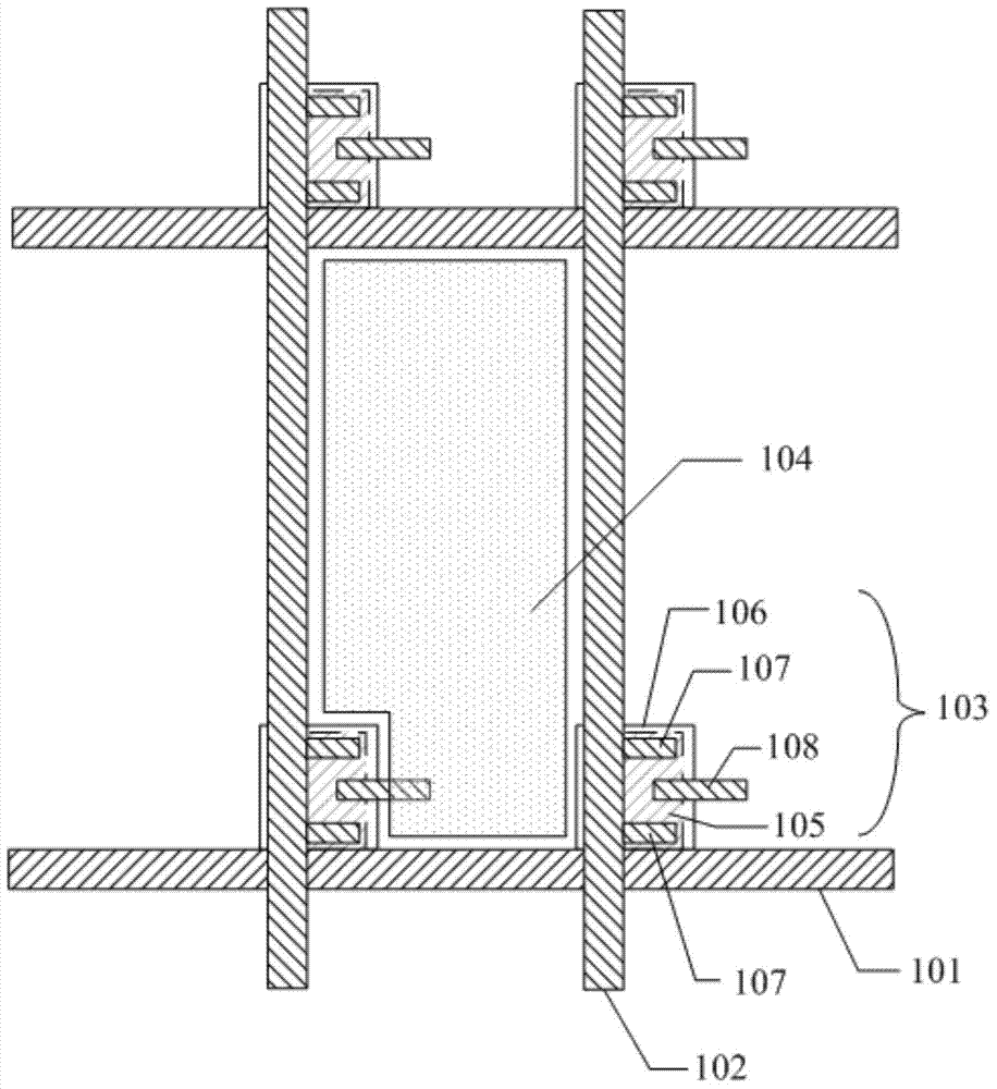
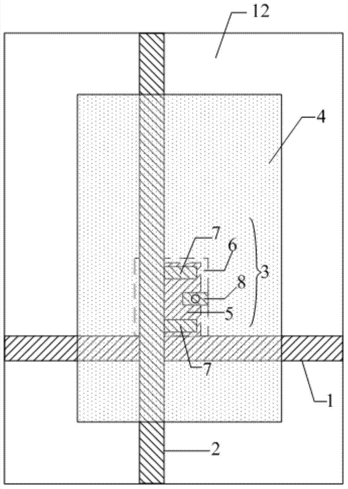
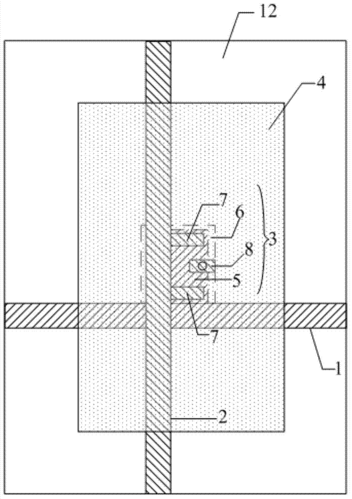
[0032] An array substrate provided by an embodiment of the present invention, such as figure 2 As shown, it includes: a base substrate, and gate lines 1 and data lines 2 ( figure 2 Take the gate line and the data line as an example), a plurality of thin film transistors 3 and a plurality of pixel electrodes 4 corresponding to the thin film transistors 3 ( figure 2 Take one of the thin film transistors and the corresponding pixel electrode as an example); wherein, each thin film transistor 3 includes a gate 5 and an active layer 6 that are insu...


PUM


Abstract

The invention discloses an array substrate and a display device. The array substrate comprises a substrate body, a plurality of thin-film transistors and a plurality of pixel electrodes, the thin-film transistors and the pixel electrodes are located on the array substrate, and the thin-film transistors correspond to the pixel electrodes one to one. Because the orthographic projection, on the substrate body, of each thin-film transistor is completely located within the orthographic projection, on the substrate body, of the corresponding pixel electrode, when gray scale signals loaded on data lines charge the pixel electrodes through the thin-film transistors, charging can be carried out from the interior to the periphery of each pixel electrode, the pixel electrodes can be fast charged, the charging efficiency of the pixel electrodes can be improved, and the response speed of a flat-panel display can be increased.

Description

technical field [0001] The present invention relates to the field of display technology, in particular to an array substrate and a display device. Background technique [0002] With the continuous development of display technology, light emitting diode (Light Emitting Diode, LED), organic light emitting diode (Organic Light Emitting Diode, OLED), plasma display (Plasma Display Panel, PDP) and liquid crystal display (Liquid Crystal Display, LCD) etc. Flat panel displays are developing rapidly. [0003] Array substrates in existing flat panel displays, such as figure 1 As shown, it includes: a base substrate, and a gate line 101, a data line 102, a thin film transistor (Thin Film Transistor, TFT) 103 and a pixel electrode 104 located on the base substrate; the thin film transistor 103 generally includes a gate 105, an active layer 106 , source 107 and drain 108 , wherein the gate 105 is connected to the gate line 101 , the source 107 is connected to the data line 102 , and t...

Claims


Application Information

Patent Timeline
Patent Type & Authority Applications(China)
IPC IPC(8): H01L27/12G02F1/1343G02F1/1368
Inventor 马俊才
Owner HEFEI BOE OPTOELECTRONICS TECH
Why Eureka
Try Eureka