Organic single-crystal spinning diode and manufacturing method thereof

A diode and single crystal technology, applied in the field of organic single crystal spin diodes and its preparation, can solve the problems of reduced spin diffusion length of materials, electron traps, low yield rate, etc.

Inactive Publication Date: 2015-01-07
SHANDONG UNIV
View PDF2 Cites 4 Cited by
  • Summary
  • Abstract
  • Description
  • Claims
  • Application Information

AI Technical Summary

Problems solved by technology

Since then, there have been many studies on organic spintronic devices, but the organic layers of the devices are basically amorphous or microcrystalline thin films, and there are a large number of electronic traps, defects, impurities and other factors inside, which greatly reduce the spin diffusion length of the material.
The diffusion length of the organic layer is only tens of nanometers, which has extremely high requirements on the preparation process of the device, resulting in a low yield rate

Method used


Image

  • Organic single-crystal spinning diode and manufacturing method thereof
  • Organic single-crystal spinning diode and manufacturing method thereof

Examples


Embodiment 1

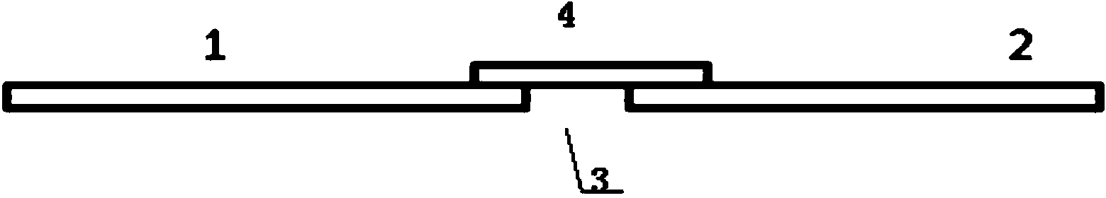
[0027] An organic single crystal spin diode, comprising two ferromagnetic electrodes, a micron-scale channel 3 is arranged between the two ferromagnetic electrodes, the channel 3 is covered with a transport layer, and the transport The layer is an organic semiconducting single crystal 4 connecting the two ferromagnetic electrodes. The organic semiconductor single crystal is an organic semiconductor compound single crystal in which rubrene has a planar molecular structure. The width of the channel is 2 μm.

Embodiment 2

[0029] An organic single crystal spin diode as described in Embodiment 1, the difference is that the organic semiconductor single crystal is a porphyrin compound organic semiconductor single crystal.

Embodiment 3

[0031] An organic single crystal spin diode as described in Embodiment 1, the difference is that the organic semiconductor single crystal is a phthalocyanine metal complex organic semiconductor single crystal.


PUM


Abstract

The invention provides an organic single-crystal spinning diode. The organic single-crystal spinning diode comprises two ferromagnetic electrodes. A micron-order channel is formed between the two ferromagnetic electrodes and covered with a transmission layer. The transmission layer is an organic semiconductor single crystal which is connected with the two ferromagnetic electrodes. The organic single crystal is adopted due to the fact that the structure of the organic single crystal is single, the quality of the crystal is good, defects, impurities, crystal boundaries and other influence factors can be avoided to the maximum degree, and the material spinning diffusion length can be increased to a large degree. Along with the increase of the carrier spinning diffusion length, the manufacturing difficulty of organic spinning electronic and photoelectronic devices can be lowered, and the important promoting effect on development of organic spinning electronics and organic spinning photoelectronics is achieved. Meanwhile, an organic single-crystal device with the large-distance organic transmission layer is manufactured, the influences of an external magnetic field on device characteristics are observed, and a certain experimental basis is provided for the research on the production mechanism of an organic magnetic resistor.

Description

technical field [0001] The invention relates to an organic single crystal spin diode and a preparation method thereof, belonging to the technical field of spin electronics. Background technique [0002] Spintronics has received a lot of attention in scientific research in recent years. The emergence of spintronics combines the spin characteristics of electrons with the charge characteristics, and is usually used to study the spin injection, spin transport, spin detection and spin regulation of electrons in devices. Therefore, the characteristics of the device in optics, electricity, and magnetism are combined to obtain a new type of spintronic device. [0003] Compared with inorganic semiconductors, organic semiconductors have the characteristics of weak spin-orbit coupling and hyperfine interaction, long carrier spin relaxation time, and good combination with flexible substrates. They have good applications in spintronics. Value. Organic materials have a very long spin r...

Claims


Application Information

Patent Timeline
Patent Type & Authority Applications(China)
IPC IPC(8): H01L51/10H01L51/30H01L51/40
CPCH10K85/311H10K85/321H10K10/00H10K10/82
Inventor 庞智勇宋辉赵宇谢万峰韩圣浩
Owner SHANDONG UNIV
Why Eureka
Try Eureka