Detection circuit, liquid crystal display panel and manufacturing method of liquid crystal display panel

A liquid crystal display panel and detection circuit technology, applied in nonlinear optics, instruments, optics, etc., can solve the problems of scanning line or data line signal interference, affecting panel display effect, voltage characteristic curve drift, etc., to reduce leakage risk, The effect of ensuring the quality of the screen display

Inactive Publication Date: 2015-01-14
TCL CHINA STAR OPTOELECTRONICS TECH CO LTD
View PDF4 Cites 22 Cited by
  • Summary
  • Abstract
  • Description
  • Claims
  • Application Information

AI Technical Summary

Problems solved by technology

For the case where thin film transistors are used as control switches (such as figure 1 As shown), when the display panel is working normally, the gate of the thin film transistor needs to be in a negative bias state for a long time, and its voltage characteristic curve (I-V Curve) may drift
At the same time, since the test short-circuit ring or short-circuit bar is suspended for a long time, its potential is easily disturbed and fluctuates greatly. Therefore, the conductive channel between the drain and source of the thin film transistor cannot be completely closed, and a leakage channel will be formed. Furthermore, different scanning lines or data lines form a leakage path ( figure 1 The dotted line shown), which causes the signals of different scan lines or data lines to interfere with each other, affecting the display effect of the panel

Method used


Image

  • Detection circuit, liquid crystal display panel and manufacturing method of liquid crystal display panel
  • Detection circuit, liquid crystal display panel and manufacturing method of liquid crystal display panel
  • Detection circuit, liquid crystal display panel and manufacturing method of liquid crystal display panel

Examples


Embodiment Construction

[0030] In order to improve the leakage phenomenon between the signal lines inside the panel without affecting the work, the present invention further improves the detection circuit of the liquid crystal display panel in the prior art. The technical solution of the present invention and the technical effects that can be achieved will be described in detail below in conjunction with non-limiting embodiments and with reference to the accompanying drawings.

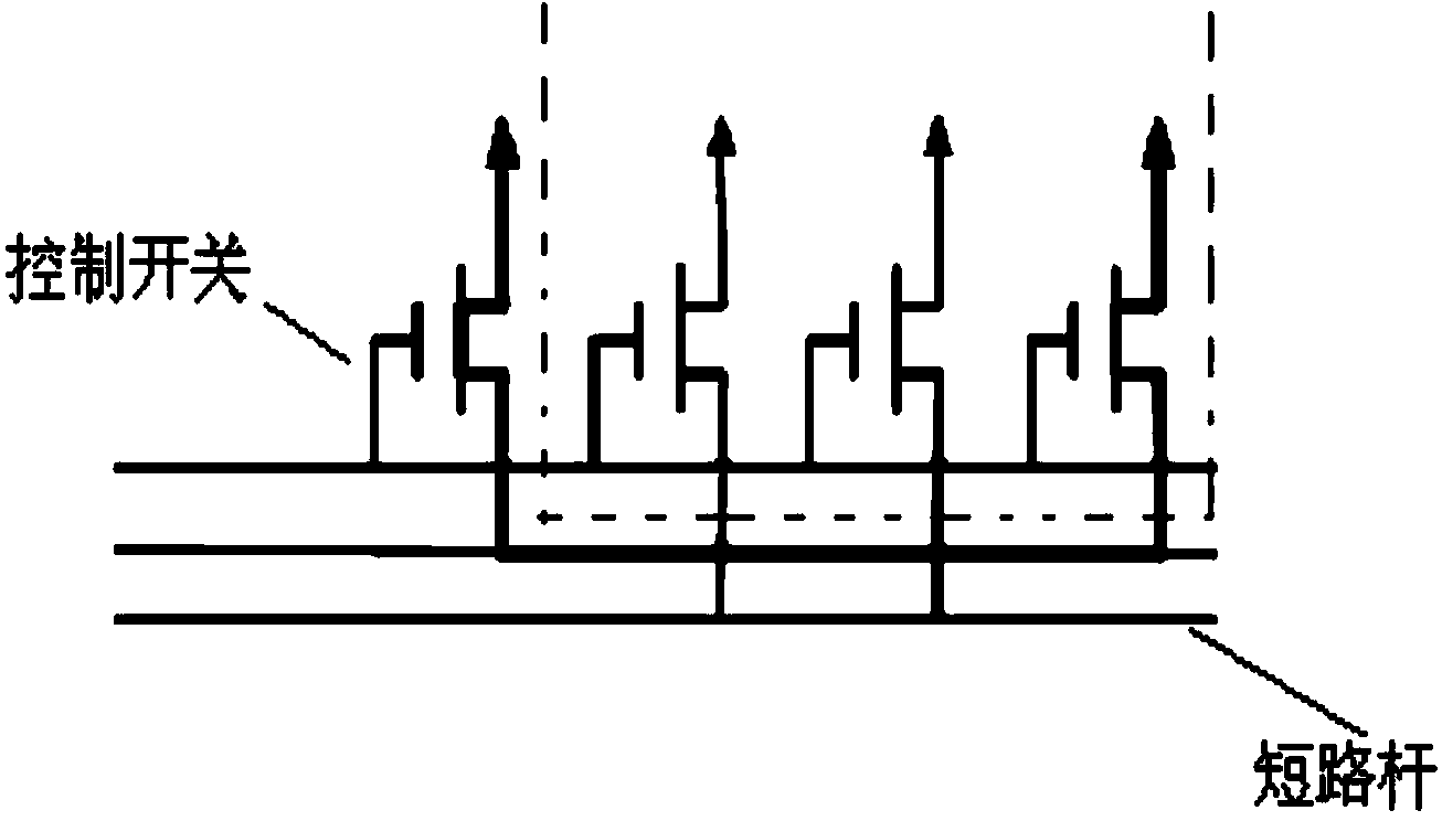
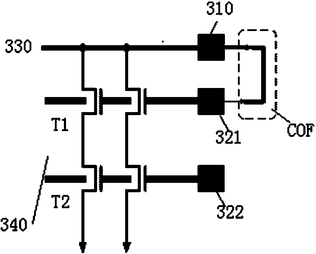
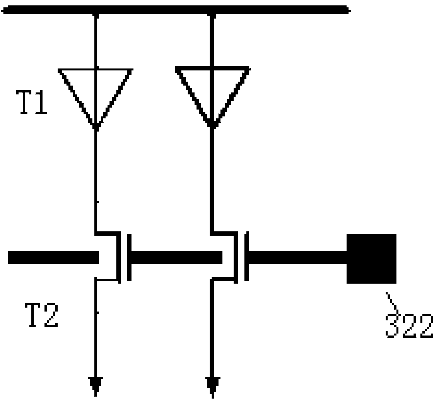
[0031] Same as the prior art, in this embodiment, the liquid crystal display panel to be tested includes a thin film transistor array substrate and a color filter substrate. Wherein, the thin film transistor array substrate is divided into two major areas, a display area and a non-display area. The display area of ​​the thin film transistor array substrate includes a plurality of pixel areas formed by a plurality of scanning lines and data lines interlaced. Each pixel area is provided with a pixel unit, and each pixel unit i...


PUM


Abstract

The invention relates to a detection circuit, a liquid crystal display panel and a manufacturing method of the liquid crystal display panel. The detection circuit comprises a control switch unit which is arranged between a test signal input end and liquid crystal display panel signal lines and comprises a first switch transistor and a second switch transistor. In the period of detection, the first switch transistor and the second switch transistor are kept on, and a test signal is enabled to enter the liquid crystal display panel signal lines; after detection, the second switch transistor is kept off, the control end of the first switch transistor is in short-circuit connection with the first end, and accordingly leakage current flowing into the liquid crystal display panel signal lines from the second switch transistor is reduced. By the liquid crystal display panel with the detection circuit, risk of electric leakage between the signal lines in the panel is lowered effectively under the condition that operation is unaffected, and image display quality is ensured.

Description

technical field [0001] The invention relates to a liquid crystal display panel manufacturing process, in particular to a detection circuit, a liquid crystal display panel and a manufacturing method thereof. Background technique [0002] In the production process of liquid crystal display panels (LCD Panel), it is necessary to perform electrical testing (Cell Test) on the thin-film transistor array substrate to test whether the thin-film transistors on the array substrate that control the operation of each pixel unit are operating normally, so as to pick out abnormal ones. For array substrates, defective products are eliminated in time before the subsequent production process. The detection circuit used for electrical measurement is usually arranged in the non-display area of ​​the array substrate, and has two common wiring methods: short ring layout and short bar layout. Whether it is the detection circuit of the ring-shaped short-circuit wiring or the detection circuit of ...

Claims


Application Information

Patent Timeline
Patent Type & Authority Applications(China)
IPC IPC(8): G02F1/13G02F1/1333
CPCG02F1/1309G02F1/133351G02F1/136254G02F1/13G02F1/1333G02F1/133514G02F1/136286G02F1/1368G02F2203/69
Inventor 杜鹏施明宏
Owner TCL CHINA STAR OPTOELECTRONICS TECH CO LTD
Why Eureka
Try Eureka