High-voltage static protection structure

A technology for protecting structures and high-voltage static electricity, which is applied to circuits, electrical components, and electric solid devices. The effect of capacity improvement

Active Publication Date: 2015-01-14
SHANGHAI HUAHONG GRACE SEMICON MFG CORP
View PDF4 Cites 4 Cited by
  • Summary
  • Abstract
  • Description
  • Claims
  • Application Information

AI Technical Summary

Problems solved by technology

The turn-on of the triode is mainly triggered by the junction breakdown between the N-diffusion region and the high-voltage P-well. Such a trigger voltage is generally relatively high, and the snapback voltage is very low, and it is not easy to adjust, and it is easy to trigger the latch-up effect.

Method used


Image

  • High-voltage static protection structure
  • High-voltage static protection structure

Examples


Embodiment Construction

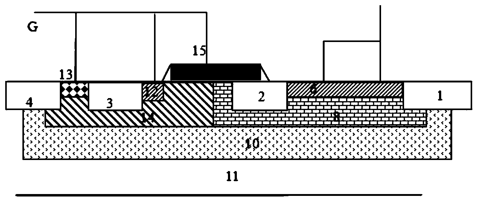
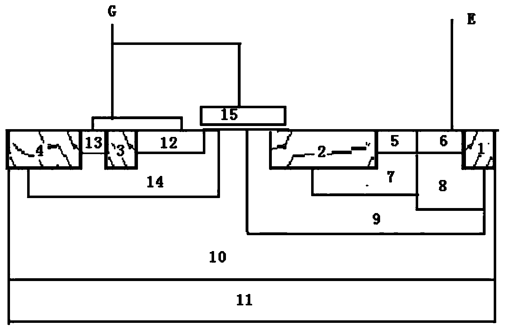
[0031] An embodiment of the present invention includes: an N-type LDMOS is placed entirely in the N-type buried layer 10 above a silicon substrate 11; the active region on the right side of the polysilicon gate 15 is the drain region of the LDMOS, and the drain region Including the first P+ diffusion region 5 and the P- implantation region 7 below it, the first N+ diffusion region 6 and the N- implantation region 8 below it, the first P+ diffusion region 5 and the first N+ diffusion region 6 are adjacent , the P-implantation region 7 is adjacent to the N-implantation region 8; the first N+ diffusion region 6 has a first field oxygen region 1 on the side away from the polysilicon gate 15, and the first P+ diffusion region 5 is close to a side of the polysilicon gate 15 The side has a second field oxygen region 2;

[0032] The active region on the left side of the polysilicon gate 15 is the source region of the N-type LDMOS, and the source region includes the second N+ diffusion...


PUM


Abstract

The invention discloses a high-voltage static protection structure. The high-voltage static protection structure comprises an N-type LDMOS which is arranged in an N-type buried layer on a silicon substrate; an active region on the right side of a polycrystalline silicon gate is a drain region of the LDMOS, and is composed of a high-voltage N trap, a P-type injection region, an N-type injection region, a first P+ type diffusion zone and a first N+ type diffusion zone; the P-type injection region is arranged below the first P+ type diffusion zone and part of a field oxidation region, the N-type injection region is arranged below the first N+ type diffusion zone, and the P-type injection region and the N-type injection region are surrounded by the high-voltage N trap; an active region on the left side of the polycrystalline silicon gate is a source region of the N-type LDMOS and is composed of a second N+ type diffusion zone; a second P+ type diffusion zone is arranged between the second N+ type diffusion zone and a third field oxidation zone; the first N+ type diffusion zone of the drain region is connected with an ESD inlet end, and the second N+ type diffusion zone, the second P+ type diffusion zone and the polycrystalline silicon gate of the source region are jointly connected with the ground. By means of the high-voltage static protection structure, the even conduction capacity can be improved, and the snapback voltage can be improved for preventing the latch-up effect.

Description

technical field [0001] The invention relates to the field of semiconductor manufacturing, in particular to a high-voltage electrostatic protection structure for electrostatic protection. Background technique [0002] Electrostatic discharge (ESD) damage to electronic products has always been a problem that is not easy to solve. For high-voltage processes, electrostatic protection devices not only need to meet the requirements that the withstand voltage is greater than the power supply voltage, but their electrostatic trigger voltage also needs to be lower than the damage of the protected device. Voltage is fine. Such as figure 1 As shown, in an existing high-voltage NLDMOS structure used for electrostatic protection, under the occurrence of static electricity, ESD positive charges enter the drain of the structure from the input and output pads, and raise the potential of the N-diffusion region, causing avalanche breakdown and breakdown. The current is extracted through the...

Claims


Application Information

Patent Timeline
Patent Type & Authority Applications(China)
IPC IPC(8): H01L23/60H01L29/78H01L29/417
Inventor 苏庆邓樟鹏苗彬彬张强
Owner SHANGHAI HUAHONG GRACE SEMICON MFG CORP
Why Eureka
Try Eureka