

High-voltage electrostatic protection structure
A protection structure, high-voltage electrostatic technology, applied in circuits, electrical components, electrical solid devices, etc., can solve the problems of high trigger voltage and not easy to play a protective role.
- Summary
- Abstract
- Description
- Claims
- Application Information
AI Technical Summary
Problems solved by technology
Method used
Image

Examples
Embodiment Construction
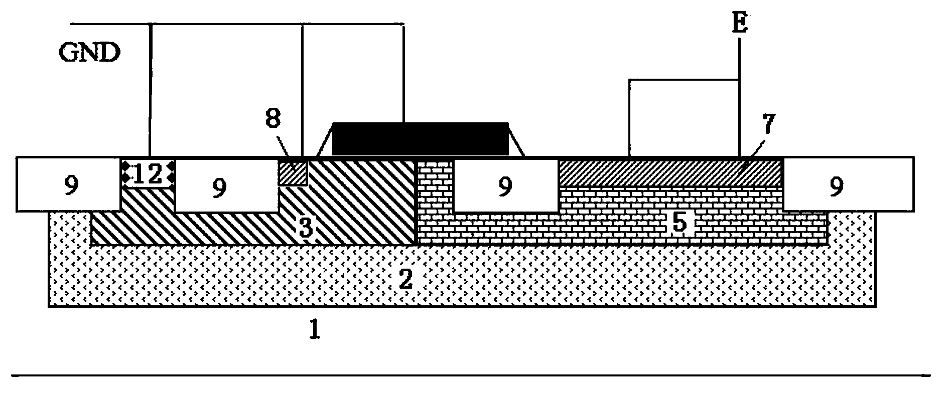
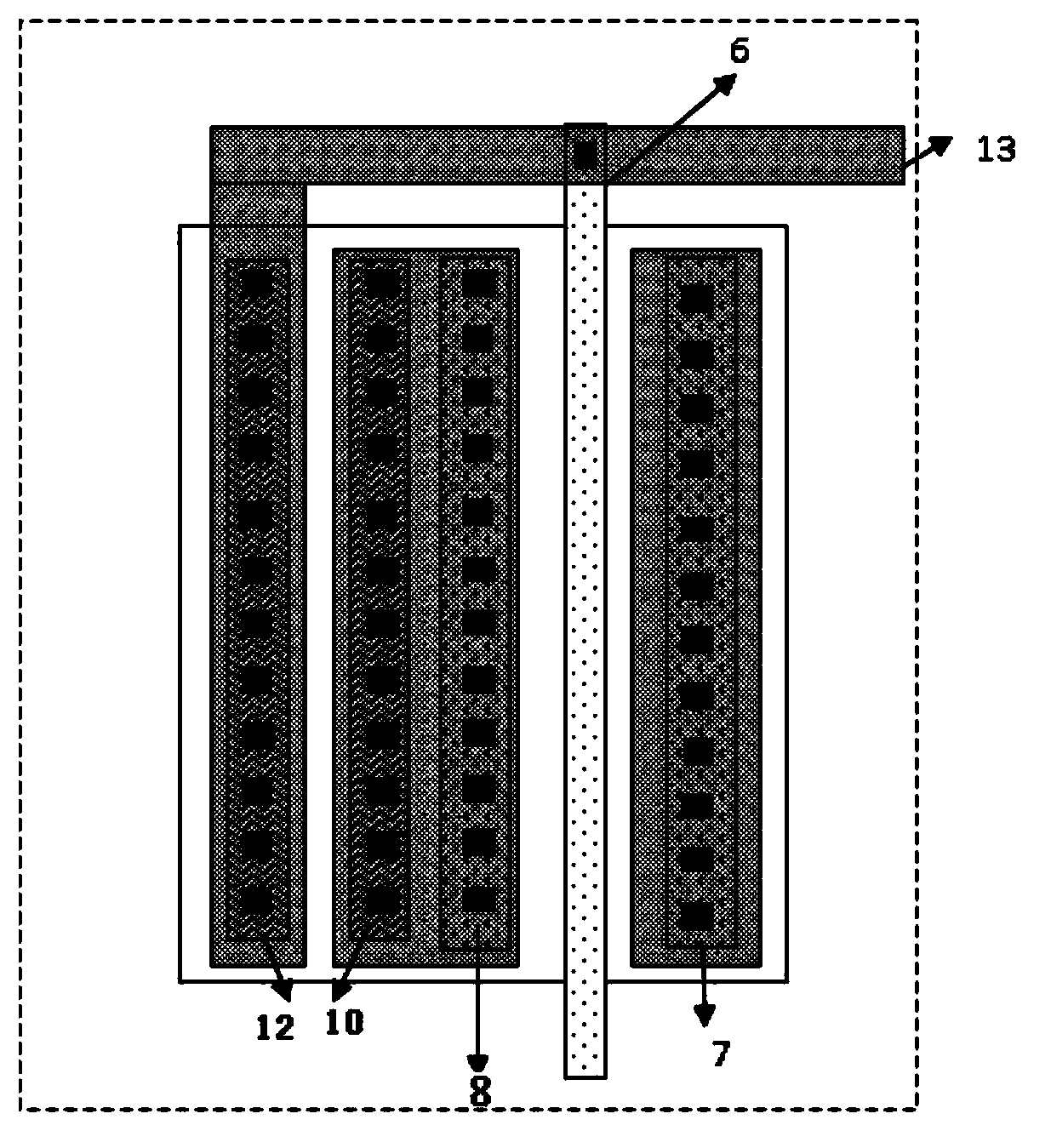
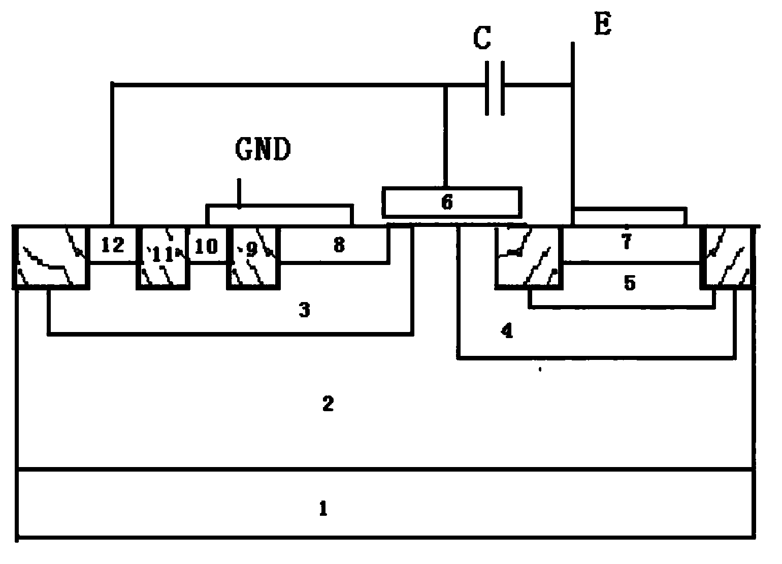
[0025] Such as figure 2 , image 3 As shown, an embodiment of the present invention includes: an N-type LDMOS is placed entirely in an N-type buried layer 2 above a silicon substrate 1; the active region on the right side of the polysilicon gate 6 of the LDMOS device is the device The drain region, which is connected to the ESD entry end, has an N+ implant region 7, an N- implant region 5 and a high-voltage N well 4 below the drain region; the active region on the left side of the polysilicon gate is the source region of the device , there is an N+ type implant region 8 below the source region, a first P type active region 10 is isolated on the left side of the N+ type implant region 8 adjacent to the field oxygen region 9, and on the left side of the first P type active region 10 A second P-type active region 12 is isolated from the adjacent field oxygen region 11;
[0026] The drain region of the LDMOS device is connected to the ESD entry end, the source region is grounde...
PUM
 Abstract
Description
Claims
Application Information