High voltage electrostatic protection structure
A protection structure, high-voltage electrostatic technology, applied in circuits, electrical components, electro-solid devices, etc., can solve the problems of low snapback voltage, high trigger voltage, difficult to adjust, etc., to improve the snapback voltage and electrostatic discharge capacity. Effect
- Summary
- Abstract
- Description
- Claims
- Application Information
AI Technical Summary
Problems solved by technology
Method used
Image
Examples
Embodiment Construction
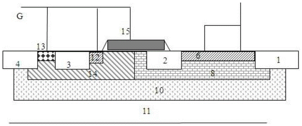
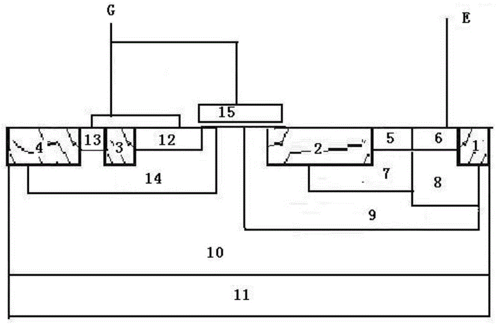
[0031] An embodiment of the present invention includes: an N-type LDMOS is placed entirely in the N-type buried layer 10 above a silicon substrate 11; the active region on the right side of the polysilicon gate 15 is the drain region of the LDMOS, and the drain region Including the first P+ diffusion region 5 and the P- implantation region 7 below it, the first N+ diffusion region 6 and the N- implantation region 8 below it, the first P+ diffusion region 5 and the first N+ diffusion region 6 are adjacent , the P-implantation region 7 is adjacent to the N-implantation region 8; the first N+ diffusion region 6 has a first field oxygen region 1 on the side away from the polysilicon gate 15, and the first P+ diffusion region 5 is close to a side of the polysilicon gate 15 The side has a second field oxygen region 2;
[0032] The active region on the left side of the polysilicon gate 15 is the source region of the N-type LDMOS, and the source region includes the second N+ diffusion...
PUM
 Abstract
Description
Claims
Application Information

