Highly integrated high mobility source-drain gate-assisted junction-free transistor

A junctionless transistor, high-mobility technology, applied in semiconductor devices, electrical components, circuits, etc., can solve the problems of decreased device mobility, influence on device turn-on characteristics, and influence on device reliability, to increase the effective channel length, The effect of overcoming short channel effect and low source-drain resistance

Inactive Publication Date: 2017-07-21
SHENYANG POLYTECHNIC UNIV
View PDF5 Cites 0 Cited by
  • Summary
  • Abstract
  • Description
  • Claims
  • Application Information

AI Technical Summary

Problems solved by technology

However, such a highly doped channel will lead to a significant decrease in the mobility of the device, and the random scattering of impurities will seriously affect the reliability of the device.
In order to improve the mobility and reliability of junctionless devices, it is necessary to reduce the doping concentration of the silicon film, but the reduction of the doping concentration will increase the source-drain resistance and affect the turn-on characteristics of the device
In addition, the common transistor structure based on the planar structure, with the continuous shortening of the channel length, the short channel effect is gradually enhanced, and the device is difficult to turn off

Method used


Image

  • Highly integrated high mobility source-drain gate-assisted junction-free transistor
  • Highly integrated high mobility source-drain gate-assisted junction-free transistor
  • Highly integrated high mobility source-drain gate-assisted junction-free transistor

Examples


Embodiment Construction

[0027] Below in conjunction with accompanying drawing, the present invention will be further described:

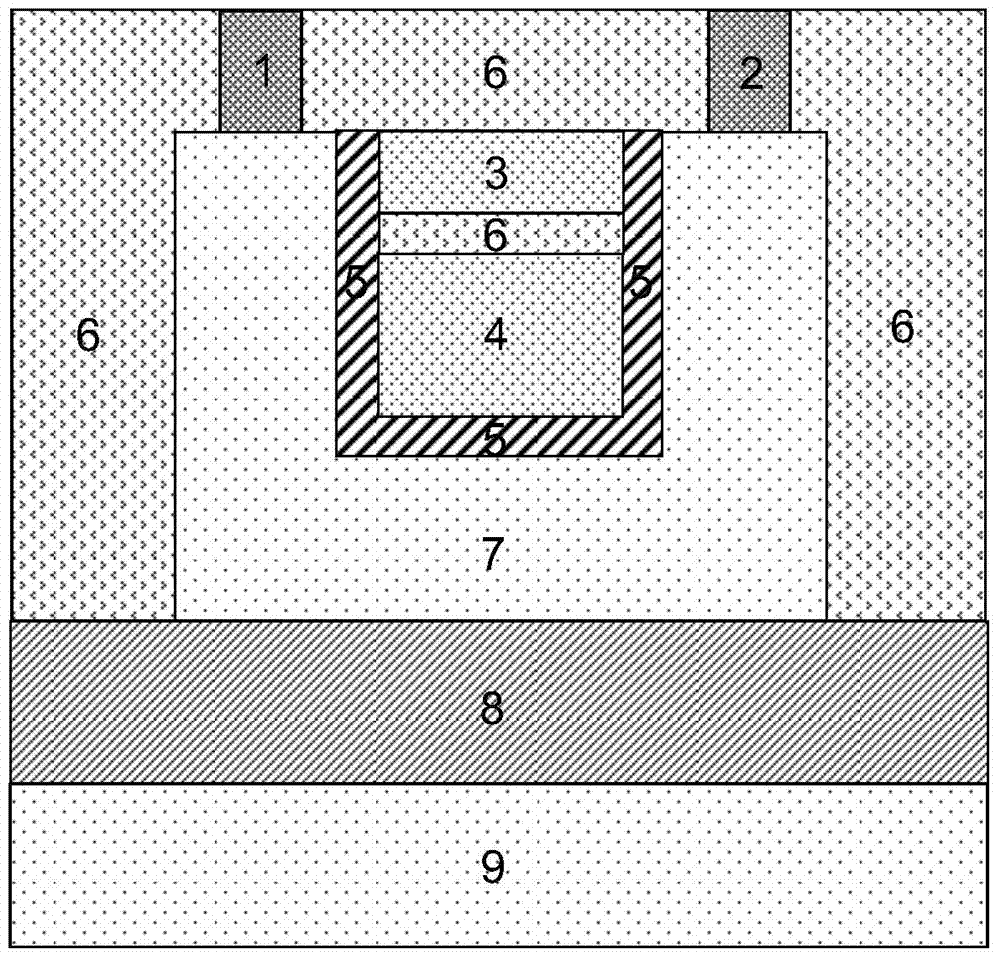
[0028] The high-integration, high-mobility source-drain-gate assisted junction-free transistor of the present invention, through the joint action of the source-drain control gate electrode 3 and the gate electrode 4, which are independently controlled electrodes, can be used under the condition of low doping concentration. A junction-free transistor with high mobility and low source-drain resistance is realized. Taking the N-type as an example, when the device is working, the source-drain control gate electrode 3 always maintains a constant high potential, so that the left and right sides of the source-drain control gate electrode 3 correspond to the single crystals under the source electrode 1 and the drain electrode 2 respectively. The left and right ends of the silicon groove 7 form electron accumulation, and the accumulated electrons enhance the conductivity of the lef...


PUM


Abstract

The invention relates to a high-integration, high-mobility source-drain-gate assisted junction-free transistor, which adopts two independently controlled gate electrodes, such as a source-drain control gate electrode and a gate electrode, so that the device can be guaranteed at a low doping concentration. High mobility can be achieved in the channel, avoiding the decline of device mobility and stability caused by the enhancement of random scattering effect under high doping concentration, and at the same time, a lower source can be obtained through the independent control of the source-drain control gate electrode and the gate electrode. Leakage resistance, thus effectively solving the contradiction between the increase of the source-drain resistance caused by the low doping concentration of the channel of ordinary junctionless transistors, and the high doping concentration will lead to the decrease of device mobility and stability. In addition, by adopting the groove-shaped channel design, compared with the ordinary planar structure, the effective channel length is significantly increased without increasing the additional chip area to reduce the short channel effect of the device at the deep nanoscale, so it is suitable for Promote apps.

Description

technical field [0001] The invention belongs to the field of ultra-large-scale integrated circuit manufacturing, and in particular relates to a high-integration, high-mobility, source-drain-gate auxiliary-controlled junctionless transistor structure suitable for ultra-high-integration integrated circuit manufacturing. Background technique [0002] The basic unit of integrated circuits, MOSFETs, transistors, with the continuous reduction in size, need to achieve multiple orders of magnitude concentration differences within a distance of several nanometers to form extremely steep source and drain PN junctions. Such a concentration gradient is essential for doping And heat treatment process has extremely high requirements. The above problems can be effectively solved by junction-free field-effect transistors fabricated on SOI wafers. Junction-free transistors adopt multi-subconduction, and the source, drain and channel regions of the device have the same high doping concentrati...

Claims


Application Information

Patent Timeline
Patent Type & Authority Patents(China)
IPC IPC(8): H01L29/78H01L29/423H01L29/10
CPCH01L29/1037H01L29/4236H01L29/7831
Inventor 刘溪靳晓诗揣荣岩
Owner SHENYANG POLYTECHNIC UNIV
Why Eureka
Try Eureka