Mainboard debugging circuit

A technology for debugging circuits and motherboards, which is applied in electrical digital data processing, using start-up tests to detect faulty hardware, instruments, etc. Effect

Active Publication Date: 2015-01-21
嘉善县魏塘资产管理有限公司
View PDF5 Cites 7 Cited by
  • Summary
  • Abstract
  • Description
  • Claims
  • Application Information

AI Technical Summary

Problems solved by technology

In debugging, usually an interface connector connected to the main board is configured for the PCH and CPU respectively. In this way, not only the space on the main board is occupied, but also the corresponding interface connector needs to be replaced when the debugging of the PCH and the CPU is switched, resulting in Reduced debugging efficiency

Method used


Image

  • Mainboard debugging circuit
  • Mainboard debugging circuit

Examples


Embodiment Construction

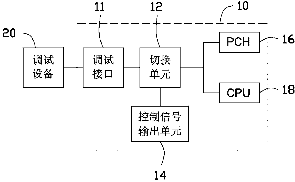
[0016] Such as figure 1 As shown, it is a block diagram of a preferred embodiment in which the motherboard debugging circuit 10 of the present invention is connected to a debugging device 20 . The motherboard debugging circuit 10 includes a debugging interface 11, a switching unit 12 connected to the debugging interface 11, a control signal output unit 14 connected to the switching unit 12, a platform control center (Platform Controller Hub) connected to the switching unit 12 , PCH) 16 and microprocessor (Central Processing Unit, CPU) 18. The switching unit 12 receives the control signal sent by the control signal output unit 14 , and selectively transmits the data signal of the platform control center 16 or the microprocessor 18 to the debugging device 20 through the debugging interface 11 .

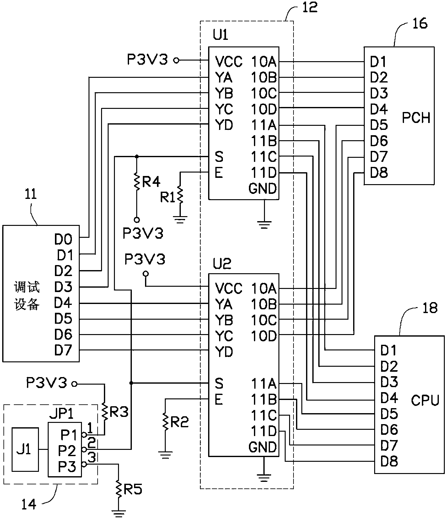
[0017] Such as figure 2 As shown, the platform control hub 16 includes a first group of data pins D1-D4 and a second group of data pins D5-D8. The microprocessor 18 includes a first...


PUM


Abstract

A debugging circuit comprises a debugging interface, a switch unit coupled to the debugging interface, a controller coupled to the switch unit, a platform controller hub (PCH), and a central processing unit (CPU). The PCH and the CPU are coupled to the switch unit. The debugging interface is coupled between the switch unit and a debugging device. The switch unit receives a control signal from the controller, and selectively outputs a first data signal from the PCH or a second data signal from the CPU to the debugging device through the debugging interface according to the control signal.

Description

technical field [0001] The invention relates to a motherboard debugging circuit. Background technique [0002] In the current server design, we need to use the Basic Input Output System (BIOS) to troubleshoot the motherboard's Platform Controller Hub (PCH) and microprocessor (Central Processing Unit, CPU). In debugging, usually an interface connector connected to the main board is configured for the PCH and CPU respectively. In this way, not only the space on the main board is occupied, but also the corresponding interface connector needs to be replaced when the debugging of the PCH and the CPU is switched, resulting in Debugging efficiency is reduced. Contents of the invention [0003] The invention provides a main board debugging circuit which enables a platform control center and a microprocessor to share one debugging interface. [0004] A motherboard debugging circuit, comprising: [0005] A platform control center, including a first set of data pins and a second s...

Claims


Application Information

Patent Timeline
Patent Type & Authority Applications(China)
IPC IPC(8): G06F11/22
CPCG06F11/273G06F11/2284
Inventor 周武阳梦良
Owner 嘉善县魏塘资产管理有限公司
Why Eureka
Try Eureka