CDM (Charged-Device-Model) electrostatic protection circuit

An electrostatic protection and circuit technology, applied in the direction of circuits, electrical components, electric solid devices, etc., can solve the problem that gate oxide is easy to be broken down

Inactive Publication Date: 2015-01-28
WUHAN XINXIN SEMICON MFG CO LTD
View PDF7 Cites 11 Cited by
  • Summary
  • Abstract
  • Description
  • Claims
  • Application Information

AI Technical Summary

Problems solved by technology

When an electrostatic pulse is generated, the gate oxide of ...

Method used


Image

  • CDM (Charged-Device-Model) electrostatic protection circuit
  • CDM (Charged-Device-Model) electrostatic protection circuit
  • CDM (Charged-Device-Model) electrostatic protection circuit

Examples


no. 1 example

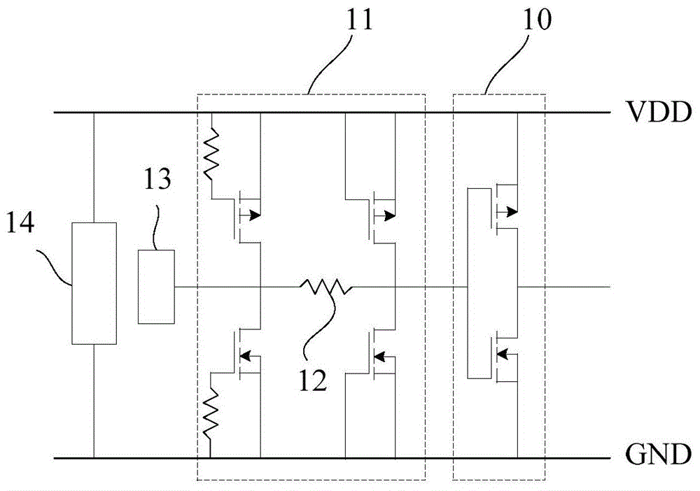
[0041] refer to Figure 4As shown, the functional unit 30 includes a PMOS transistor 301 and an NMOS transistor 302, the gate of the PMOS transistor 301 is connected to the gate of the NMOS transistor 302, and the drain of the PMOS transistor 301 is connected to the gate of the NMOS transistor 302. The drains are connected, and the gate of the PMOS transistor 301 is connected to the input / output pin 33 . The source of the PMOS transistor 301 is connected to VDD, and the source of the NMOS transistor 302 is connected to GND.

[0042] The second level protection unit 31 is GGMOS, the second level protection unit 31 includes a second PMOS transistor 311 and a second NMOS transistor 312, the drain of the second PMOS transistor 311 and the second NMOS transistor 312 The drain of the second PMOS transistor 311 is connected to VDD, the gate and source of the second NMOS transistor 312 are connected to GND.

[0043] The first level protection unit 32 is GCMOS, the first level protec...

no. 2 example

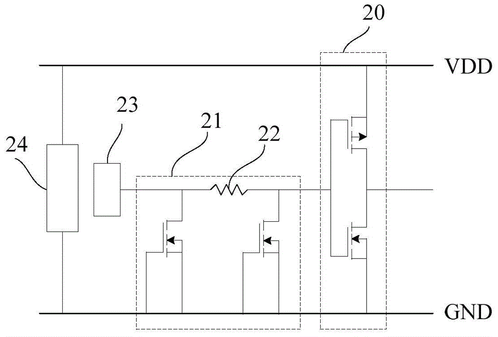
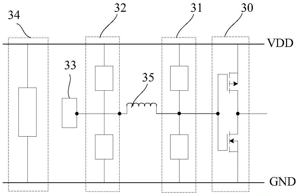
[0048] refer to Image 6 As shown, the second-level protection unit 41 and the first-level protection unit 42 adopt an open-source connection mode, the second-level protection unit 41 includes a second NMOS transistor, and the drain of the second NMOS transistor is connected to The input / output pin 43, the gate and the source of the second NMOS transistor are connected to GND. The first level protection unit 42 includes a first NMOS transistor, the drain of the first NMOS transistor is connected to the input / output pin 43 , and the gate and source of the first NMOS transistor are connected to GND. Similarly, an inductance coil 45 is connected in series between the second-level protection unit 41 and the first-level protection unit 42 . In this embodiment, the structures and connections of the functional unit 40 , the clamping circuit 44 , and the inductance coil 45 are the same as those in the first embodiment, and will not be repeated here.

[0049] In the same way, same as...


PUM


Abstract

The invention provides a CDM (Charged-Device-Model) electrostatic protection circuit. The CDM electrostatic protection circuit comprises an input and output pin, a power supply output terminal, a grounding terminal, a functional unit, a first level protection unit and a second level protection unit; the functional unit is connected with the input and output pin, the power supply output terminal and the grounding terminal; the first level protection unit is connected with the power supply output terminal and the grounding terminal; the second level protection unit is connected with the power supply output terminal and the grounding terminal; an inductance coil and a clamping circuit are connected in series between the first level protection unit and the second level protection unit; the clamping circuit is connected with the power supply output terminal and the grounding terminal. According to the CDM electrostatic protection circuit, the pulse voltage is mainly applied to two ends of the inductance coil when electrostatic pulses are produced and accordingly the voltage at two ends of each protection unit does not rapidly rise along with the electrostatic pulses and meanwhile the electrostatic pulses are released through the first level protection unit and the second level protection unit to implement the protection on the functional unit.

Description

technical field [0001] The invention relates to the design field of integrated circuit electrostatic protection circuits, in particular to a CDM electrostatic protection circuit. Background technique [0002] Integrated circuits are prone to destructive electrostatic discharge (ESD) during manufacturing, assembly and testing, or in final applications, so that integrated circuits are damaged by static electricity. [0003] ESD is typically produced by the discharge of a high voltage potential (eg, several thousand volts) and results in a short duration pulse of high current. ESD test models are usually divided into three categories. The first category is caused by the contact between human and IC. Generally, HBM (human body model) type ESD protection circuit can be made corresponding to this type of ESD. The rise time of HBM type ESD pulse is about 10ns ; The second type is caused by the contact between mechanical equipment and IC, and usually corresponding to this type of E...

Claims


Application Information

Patent Timeline
IPC IPC(8): H01L23/60
Inventor 单毅
Owner WUHAN XINXIN SEMICON MFG CO LTD
Why Eureka
Try Eureka