
Deep trench planarization methods with different structures

A planarization method and deep trench technology, applied in the direction of electrical components, semiconductor/solid-state device manufacturing, circuits, etc., can solve problems such as residue and excessive grinding surface, so as to improve yield, avoid defects, and improve the surface morphology of silicon wafers uniform effect

Active Publication Date: 2017-06-06
SHANGHAI HUAHONG GRACE SEMICON MFG CORP
View PDF5 Cites 0 Cited by
  • Summary
  • Abstract
  • Description
  • Claims
  • Application Information

AI Technical Summary

Problems solved by technology

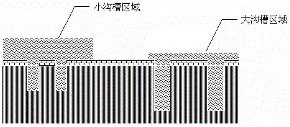
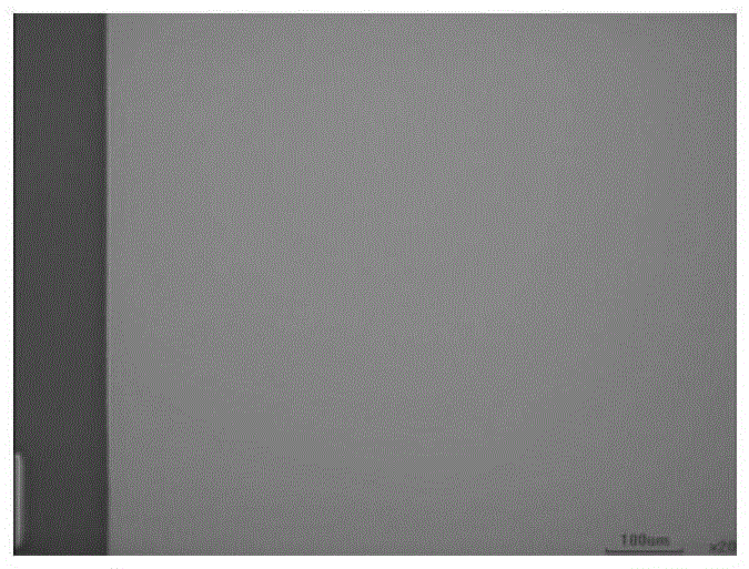
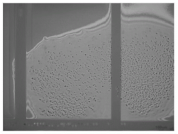
[0004] For some deep trenches with different widths and corner structures, after selective epitaxy (such as figure 1 As shown), for deep trench structures with different widths, the polysilicon thickness above the mask layer will be quite different, which will cause great challenges and difficulties to the subsequent chemical mechanical polishing process, and it is easy to cause over-polishing or surface residues. Defects (such as figure 2 , 3 shown)

Method used


Image

  • Deep trench planarization methods with different structures
  • Deep trench planarization methods with different structures
  • Deep trench planarization methods with different structures

Examples


Embodiment Construction

[0041] The deep trench planarization method with different structures of the present invention includes the steps:

[0042] 1) On the silicon substrate 1, use low pressure chemical vapor deposition (LPCVD), plasma enhanced chemical vapor deposition (PECVD) or atmospheric pressure chemical vapor deposition (APCVD) to deposit a layer with a thickness of 1000~10000 angstroms Barrier 2 (such as Figure 4 Shown);

[0043] The material of the barrier layer 2 is an oxide film (such as silicon oxide), a nitride film (such as silicon nitride), or a combination of an oxide film and a nitride film.

[0044] 2) Deposit a photoresist on the barrier layer 2. After development, dry or wet etch the barrier layer 2 to etch the barrier layer 2 to the silicon substrate 1, where the loss of the silicon substrate 1 is 100-300 Angstroms, preferably 100 Angstroms, exposing the silicon substrate 1 (such as Figure 5 Shown).

[0045] 3) On the silicon substrate 1, etch a variety of deep trench patterns with ...


PUM

PropertyMeasurementUnit
thicknessaaaaaaaaaa
depthaaaaaaaaaa
widthaaaaaaaaaa

Abstract

The invention discloses a method for flattening deep grooves with different structures. The method comprises the following steps of 1) depositing a barrier layer on a silicon substrate; 2) depositing a photoresist on the barrier layer, performing development, and etching the barrier layer to expose the silicon substrate in which a groove needs to be etched in the subsequent flow; 3) etching graphs of the deep grooves with different widths and depths on the silicon substrate; 4) filling the deep grooves of silicon by using selective epitaxial growth; 5) depositing a polycrystalline silicon buried layer on a silicon chip, wherein the polycrystalline silicon buried layer covers the surface of the whole silicon chip; 6) removing polycrystalline silicon above the barrier layer. The method has the advantages that 1) the barrier layer can be effectively protected, and a process window is added; 2) the process can be more accurately controlled in an end point detection mode by utilizing film conversion between the polycrystalline silicon and the barrier layer; 3) the surface appearance is uniform, the defects can be avoided, and the yield is improved.

Description

Technical field [0001] The present invention relates to a method for planarizing trenches in semiconductor integrated circuits, and in particular to a method for planarizing deep trenches with different structures. Background technique [0002] In today's semiconductor technology, deep trench structures are widely used. For example, as an isolation structure to isolate electronic devices with different operating voltages, and as a P-N junction in a super junction structure semiconductor device, it can achieve high breakdown voltage performance through charge balance in the depletion state. For the latter super junction metal oxide semiconductor field effect transistor (super junction MOS transistor), the method of etching and filling the deep trench during the manufacturing process is to grow an n-type epitaxial layer on an n+ type silicon substrate ( Monocrystalline silicon), then a deep trench is etched on the epitaxial layer, and then the deep trench is selectively filled wit...

Claims


Application Information

Patent Timeline
Patent Type & Authority Patents(China)
IPC IPC(8): H01L21/02H01L21/306H01L21/3105H01L21/311H01L21/336
CPCH01L21/31051
Inventor 钱志刚刘继全唐锦来
Owner SHANGHAI HUAHONG GRACE SEMICON MFG CORP
Learn More