Check patentability & draft patents in minutes with Patsnap Eureka AI!

Multi-chip mixed packaging type semiconductor device and manufacturing method thereof

A hybrid packaging and semiconductor technology, applied in semiconductor devices, semiconductor/solid-state device manufacturing, semiconductor/solid-state device components, etc., can solve the problems of increasing device thickness and ineffective heat dissipation

Active Publication Date: 2015-02-11
ALPHA & OMEGA SEMICON INT LP
View PDF7 Cites 14 Cited by
  • Summary
  • Abstract
  • Description
  • Claims
  • Application Information

AI Technical Summary

Problems solved by technology

figure 2 The disadvantage of this method is that it directly increases the final thickness of the device, and the heat dissipation effect is not increased.

Method used


Image

  • Multi-chip mixed packaging type semiconductor device and manufacturing method thereof
  • Multi-chip mixed packaging type semiconductor device and manufacturing method thereof
  • Multi-chip mixed packaging type semiconductor device and manufacturing method thereof

Examples


Embodiment Construction

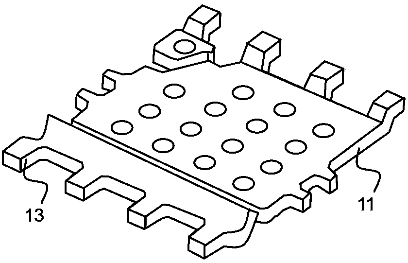
[0046] Such as Figure 3A , shows a structural schematic diagram of a chip mounting unit, usually each lead frame will contain a plurality of such units, for the sake of brief introduction, the present invention is only illustrated with one chip mounting unit. The chip mounting unit includes a first base 111, a second base 112, and first to fourth pins 101-104 that are separated from each other. The adjacent first bases 111 and second bases 112 are arranged side by side. They are roughly All are presented as square. For the convenience of description, in the plane where the chip mounting unit is located, the parallel extending direction of the first and second bases is defined as the longitudinal direction, and the separated extending direction is defined as the transverse direction. The first base 111 has a set of opposite first transverse edges 111a, second transverse edges 111b and another set of opposite first longitudinal edges 111c, second longitudinal edges 111d, and t...


PUM


Abstract

The invention relates to a power device, in particular to a thin power device with good heat radiating effect and a manufacturing method thereof. The power device comprises a chip mounting unit, a first chip, a second chip, a first interconnection structure and a second interconnection structure, wherein the first chip and the second chip are respectively adhered to a first base and a second base of the chip mounting unit, a main electrode at the front surface of the first chip and a back electrode at the back surface of the second chip are electrically connected to a fourth pin and one of a first pin and a second pin through the first interconnection structure, and an auxiliary electrode at the front surface of the first chip is electrically connected to one, which is not electrically connected with the first interconnection structure, of the first pin and the second pin through the second interconnection structure.

Description

technical field [0001] The invention generally relates to a power device, in particular to a thin power device with good heat dissipation effect and a preparation method thereof. Background technique [0002] Traditionally, the interconnection technology in power devices has various methods such as wire bonding or metal sheet connection, such as disclosed in US patent application US6870254B1 Figure 1A ~ 1C In the schematic flow diagram shown, the chip 15 is adhered on the lead frame 11, and the metal sheet 16 above the chip 15 is used to connect the electrodes of the chip 15 and the pins near the lead frame 11. The metal sheet 16 in the figure is One side is bent and extended downwards so as to be mechanically and electrically connected to a pin 13 with a V-shaped groove 18 included in the lead frame 11. This method has good heat dissipation performance when dealing with single-chip packaging, but cannot Multiple chips are packaged, because a high-end MOSFET and a low-end M...

Claims


Application Information

Patent Timeline
IPC IPC(8): H01L23/49H01L21/60
CPCH01L2224/11H01L2224/48091H01L2224/48247H01L2224/40137H01L2224/40095H01L2924/181H01L2224/40245H01L24/40H01L2224/4103H01L2224/40139H01L2924/13091H01L2224/73221H01L2224/371H01L2224/84801H01L2224/83801H01L2224/41H01L2224/37H01L2224/37013H01L2224/40H01L2224/0603H01L24/84H01L2924/00014H01L2924/00012H01L2924/00
Inventor 哈姆扎·耶尔马兹薛彦迅鲁军彼得·威尔逊霍炎牛志强鲁明朕
Owner ALPHA & OMEGA SEMICON INT LP
Features
  • R&D
  • Intellectual Property
  • Life Sciences
  • Materials
  • Tech Scout
  • Unparalleled Data Quality
  • Higher Quality Content
  • 60% Fewer Hallucinations
Learn More