Plating of a thin metal seed layer

a metal seed layer and metal layer technology, applied in the direction of electrolysis process, electrolysis components, semiconductor devices, etc., can solve the problems of void-free nanometer structures, difficult to have adequate seed step coverage with pvd techniques, and large amount of ongoing effort directed to the formation of void-free structures

Inactive Publication Date: 2005-07-07
APPLIED MATERIALS INC
View PDF99 Cites 98 Cited by
  • Summary
  • Abstract
  • Description
  • Claims
  • Application Information

AI Technical Summary

Benefits of technology

[0019] Embodiments of the invention may further provide an electrochemical plating cell configured to metallize sub 100 nanometer features on integrated circuit devices. The plating cell includes a fluid basin having an anolyte solution compartment and a catholyte solution compartment, an ionic membrane positioned between the anolyte solution compartment and the

Problems solved by technology

Many conventional deposition processes do not consistently fill semiconductor structures in which the aspect ratios exceed 6:1, and particularly when the aspect ratios exceed 10:1.
As such, there is a great amount of ongoing effort being directed to the formation of void-free, nanometer-sized structures having aspect ratios of 6:1 or higher.
However, as the feature sizes become smaller, it becomes difficult to have adequate seed step coverage with PVD techniques, as discontinuous islands of copper agglomerates are often obtained in the feature side walls close to the feature bottom.
When the deposition thickness on the field is reduced to prevent throat closure, ALD and CVD techniques are also prone to generate discontinuities in the seed

Method used


Image

  • Plating of a thin metal seed layer
  • Plating of a thin metal seed layer
  • Plating of a thin metal seed layer

Examples


Embodiment Construction

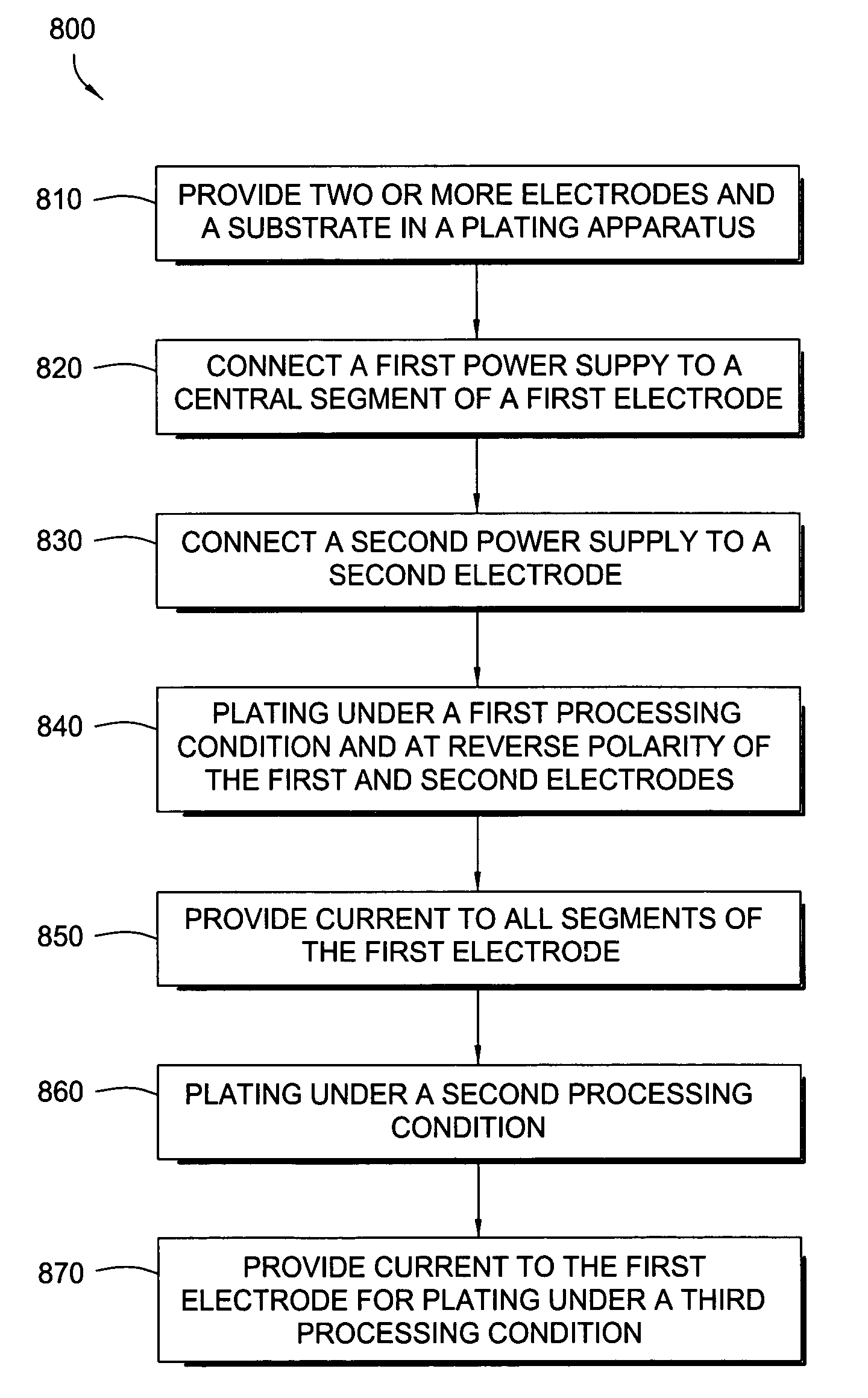
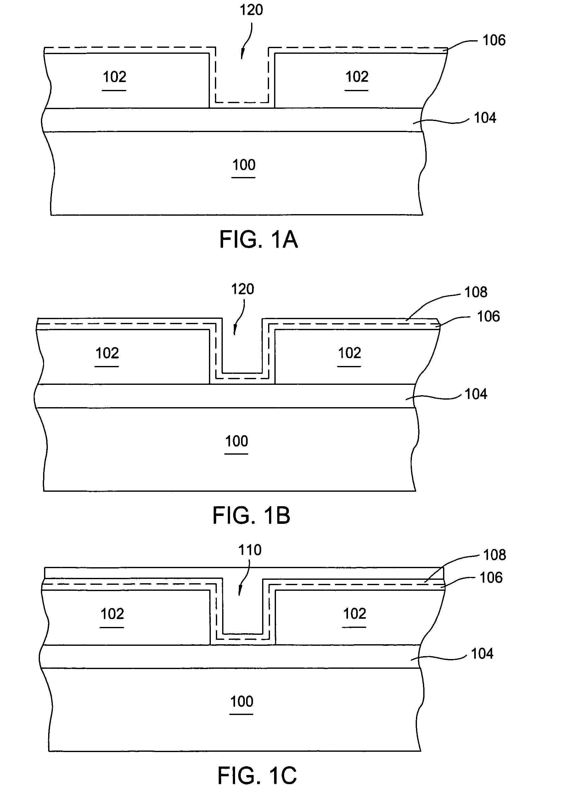
[0034] Embodiments of the invention provide a method and apparatus adapted for electrochemical deposition of a thin metal seed layer and / or a bulk metal layer on a substrate having a conductive barrier metal thereon. The metal material suitable for the bulk metal layer can be any metal materials that can be plated on a substrate surface, such as copper, nickel, etc. For example, the invention provides plating of a copper material on the surface of a barrier material or a copper seed layer during direct or indirect copper plating process to fill submicron features during semiconductor interconnect formation. In one embodiment, the invention may include at least three or more stages / steps (as will be described in detail herein) during electrochemical deposition of a conductive metal material to obtain uniform plating across the entire surface of a substrate. The three or more stages of plating can be performed in the same electrochemical deposition apparatus or in different plating to...


PUM


Abstract

A method and apparatus for plating a metal layer onto a substrate is provided. The plating apparatus includes two or more segments of an anode and an auxiliary electrode. The plating method includes a first stage of plating a thin metal seed uniformly in the center of the substrate and near the edges of the substrate before metal gap filling and bulk metal plating are performed. The thin metal seed is plated on the substrate surface by applying a current pulse provided by a first power supply and a second power supply which are in electrical communication in reverse polarity with one segment of the anode and the auxiliary electrode. Thereafter, gap filling of features is performed by applying a second current pulse where current is provided to all segments of the anode.

Description

CROSS-REFERENCE TO RELATED APPLICATIONS [0001] This application claims the benefit of U.S. provisional patent application Ser. No. 60 / 579,129, entitled “Method Of Barrier Layer Surface Treatment To Enable Direct Copper Plating”, filed on Jun. 10, 2004 and claims benefit of U.S. provisional patent application Ser. No. 60 / 621,215 (AMAT / 9201L), filed on Oct. 21, 2004, entitled “Plating Chemistry And Method Of Single-Step Electroplating Of Copper On A Barrier Metal”. This application is a continuation-in-part of co-pending U.S. patent application Ser. No. 10 / 880,103 (AMAT / 8556), titled “Multiple-Step Electrodeposition Process For Direct Copper Plating On Barrier Metals”, filed on Jun. 28, 2004; co-pending U.S. patent application Ser. No. 10 / 616,097 (AMAT / 8241), titled “Multiple-Step Electrodeposition Process For Direct Copper Plating On Barrier Metals”, filed on Jul. 8, 2003; co-pending U.S. patent application Ser. No. 10 / 664,277 (AMAT / 7735), titled “Insoluble Anode with an Auxiliary El...

Claims


Application Information

Patent Timeline
IPC IPC(8): C25D5/18
CPCC25D5/18C25D17/10H01L21/2885C25D7/123H01L21/76873H01L21/76877H01L21/76843C25D17/001C25D17/002C25D17/007
Inventor KOVARSKY, NICOLAY Y.WANG, YOUDUKOVIC, JOHN O.RODRIGUEZ, IVAN
Owner APPLIED MATERIALS INC
Why Eureka
Try Eureka