Fabrication method for high-density MRAM using thin hard mask

a fabrication method and hard mask technology, applied in the manufacture/treatment of galvano-magnetic devices, basic electric elements, electric devices, etc., can solve the problems of loss of magnetic properties, degrade and damage the magnetic properties, and the conventional method of mtj etching is reaching its limit in process capability, so as to increase the incident ibe angle

Active Publication Date: 2015-04-16
AVALANCHE TECH
View PDF3 Cites 60 Cited by
  • Summary
  • Abstract
  • Description
  • Claims
  • Application Information

AI Technical Summary

Benefits of technology

[0007]Embodiments of the invention use a thin metallic hard mask, which can be a bi-layer film, to increase the incident IBE angle for MTJ sidewall cleaning without losing the process margin for the subsequent interconnection process. The patterned metallic hard mask pads also serve as the top electrode for the MTJ cells. The thin metal hard mask, preferably approximately 10-40 nm, will increase the maximum incident angle during the IBE process that can be used to clean the re-deposited material and / or damaged material from the sidewalls of the MTJ pillars that are densely packed on the wafer. Using a thin metallic hard mask is possible when the hard mask material acts as a CMP stopper without substantial loss of thickness. In the first embodiment, the single layer hard mask is preferably ruthenium. In the second embodiment, the lower layer of the bi-layer hard mask is preferably ruthenium. The wafer is preferably rotated during the IBE process for uniform etching.

Problems solved by technology

As the device size shrinks and the cell array becomes denser, the conventional method for MTJ etching is reaching its limit in process capabilities.
However, the presence of reactive ion species during etching results in chemical reactions with MTJ layers at the sidewall of the MTJ pillar which possibly degrades and damages the magnetic properties.
However, the decrease of the MTJ feature size increases the total ratio of the damaged MTJ and can result in loss of the magnetic properties and increased magnetic property variation across the wafer as well.
However, the IBE process can be applied to the small feature size MTJ with low density but not for the high density arrays with limited pitch between two MTJ cells.
However, this IBE angle is limited by the pitch between two adjacent MTJ pillars and the height of the MTJ pillar which includes MTJ stacks and metallic hard mask.
The high incident beam angle can be used with the higher pitch, low density MTJ cells but is not usable with the small pitch for the high density MTJ cells.
Increased cell density will limit the incident angle and possibly leave re-deposited material at the sidewall.
However, this thick hard mask will limit the IBE incident beam angle for sidewall cleaning by increasing the height of the pillar.
This relatively low angle IBE process will not be sufficient to remove re-deposited and / or damaged materials from the sidewall of the MTJ during etching and could result in shorting failures which will lead to the low yields.

Method used


Image

  • Fabrication method for high-density MRAM using thin hard mask
  • Fabrication method for high-density MRAM using thin hard mask
  • Fabrication method for high-density MRAM using thin hard mask

Examples


first embodiment

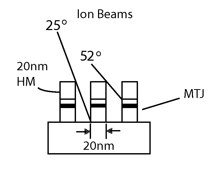
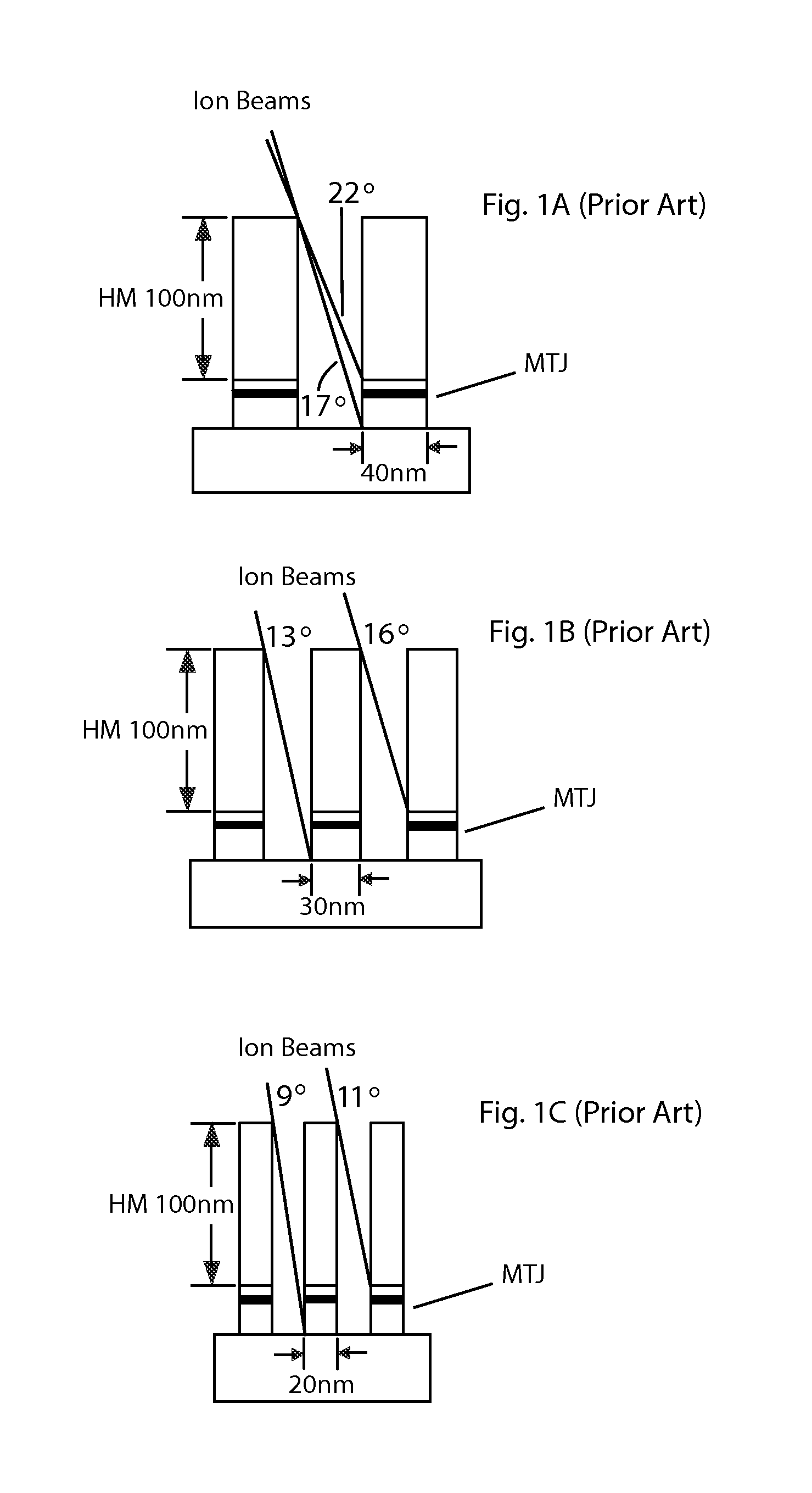
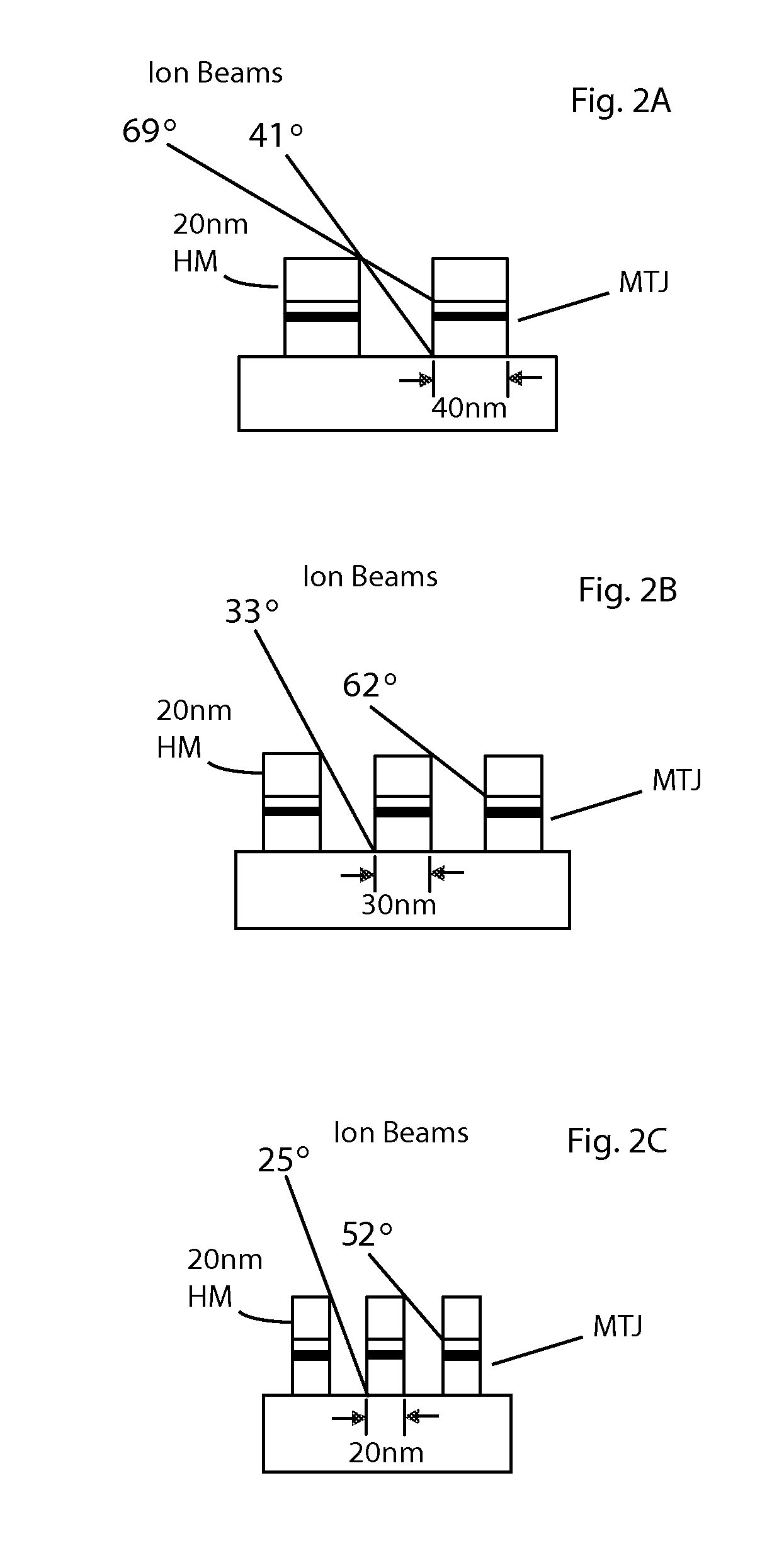
[0030]FIGS. 3 to 12 will be used to describe the first embodiment of the invention. FIG. 3 illustrates a selected stage of the MTJ and hard mask deposition process. The hard mask in the first embodiment is a single layer film, but in the second embodiment described below the hard mask includes two layers. As shown in FIG. 3 the MTJ layers have been deposited on the previously patterned control device 107 which is formed using standard techniques and is not described in this disclosure. The multiple layers in the stack for the MRAM cells have been deposited in sequence over the control device 107. The lowest layer in the cell is the bottom electrode (BE) layer 106, which is followed by the multiple layers in the MTJ stack which includes conventional layers such as the free and pinned magnetic layers and the barrier layer 104. Because the magnetic free layer, for example, can be the upper magnetic layer 103 or the lower magnetic layer 105 according to standard MTJ principles, the foll...

second embodiment

[0041]FIGS. 13 to 15 illustrate the second embodiment of the invention. In this embodiment bi-layer hard mask films are used instead of single hard mask film compared to the first embodiment. The upper layer in the bi-layer hard mask structure is totally removed during processing, but the lower layer becomes the top electrode pads. FIG. 13 illustrates that the MTJ is deposited on the control device 207 which is not described herein. The multiple layers in the stack for the MRAM cell have been deposited in sequence over the control device 207. The lowest layer in the cell is the bottom electrode (BE) layer 206, which is followed by the MTJ stack deposition in the sequence of bottom magnetic layer 205, tunnel barrier layer 204 and top magnetic layer 203. The MTJ is covered with capping layer 202, which should be a metallic material which has some selectivity during hard mask bi-layer etching. The hard mask is preferably ruthenium; therefore, Ta, Ti, TiN, TaN, W, WN, Cr, and Al are pos...


PUM

PropertyMeasurementUnit
sizeaaaaaaaaaa
thicknessaaaaaaaaaa
thicknessaaaaaaaaaa

Abstract

Embodiments of the invention are described that use a thin metallic hard mask, which can be a bi-layer film, to increase the incident IBE angle for MTJ sidewall cleaning without losing the process margin for the subsequent interconnection process. The patterned metallic hard mask pads also serve as the top electrode for the MTJ cells. Using a thin metallic hard mask is possible when the hard mask material acts as a CMP stopper without substantial loss of thickness. In the first embodiment, the single layer hard mask is preferably ruthenium. In the second embodiment, the lower layer of the bi-layer hard mask is preferably ruthenium. The wafer is preferably rotated during the IBE process for uniform etching. A capping layer under the hard mask is preferably used as the etch stopper during hard mask etch process in order not to damage or etch through the upper magnetic layer.

Description

FIELD OF THE INVENTION[0001]The present invention relates generally to designs and fabrication methods for non-volatile magnetic random access memory (MRAM) and particularly to methods for fabricating resistive memory cells in high density arrays incorporating a small feature size with minimized pitch for magnetic tunnel junction (MTJ).BACKGROUND[0002]The memories such as RRAM (Resistive Random Access Memory), PRAM (Phase Change Random Access Memory) and MRAM (Magnetic Random Access Memory) have a resistive device as a memory element. The high speed access and the non-volatility at power off of these devices make these promising technologies to replace existing memories.[0003]The resistive memory devices consisting of a top electrode, a bottom electrode and the resistive memory element in between are fabricated in an array of pillar shapes on a wafer using a conventional lithography and dry etching process. A memory element MTJ (Magnetic Tunnel Junction) in an MRAM cell includes at ...

Claims


Application Information

Patent Timeline
Patent Type & Authority Applications(United States)
IPC IPC(8): H01L43/12
CPCH01L43/12H10B61/00H10N50/01
Inventor JUNG, DONG HASATOH, KIMIHIROZHANG, JINGZHOU, YUCHENHUAI, YIMING
Owner AVALANCHE TECH
Why Eureka
Try Eureka