Multibit metal nanocrystal memories and fabrication

a metal nanocrystal and memory technology, applied in the field of multi-bit metal nanocrystals, can solve the problems of difficult fabrication of high-density drams, high power consumption of constant refresh operations, flash memories with longer than 10 years of retention time, etc., and achieve the effect of improving the performance of memory cell devices

Active Publication Date: 2007-08-21
CORNELL RES FOUNDATION INC
View PDF14 Cites 60 Cited by
  • Summary
  • Abstract
  • Description
  • Claims
  • Application Information

AI Technical Summary

Benefits of technology

[0005]In accordance with the present invention, metal nanocrystal memories are utilized to further enhance the performance of memory cell devices through work-function engineering. The electrical characterization of metal nanocrystal memories, for both single and multi-bit operations, is described herein, as is

Problems solved by technology

DRAMs allow fast write/erase, but suffer from high power consumption incurred by the constant refresh operations due to their short retention time of less than a few seconds (see B. El-Kareh et al, “The Evolution of DRAM Cell Technology”, Solid State Technology, Vol. 40, pp 89, May 1997).
It is also very difficult to fabricate high-density DRAMs, because a large capacitor is necessary f

Method used


Image

  • Multibit metal nanocrystal memories and fabrication
  • Multibit metal nanocrystal memories and fabrication
  • Multibit metal nanocrystal memories and fabrication

Examples


Embodiment Construction

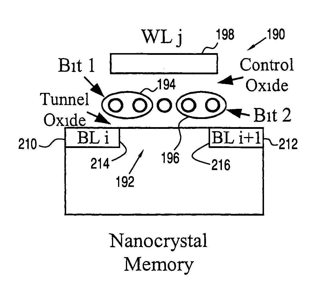
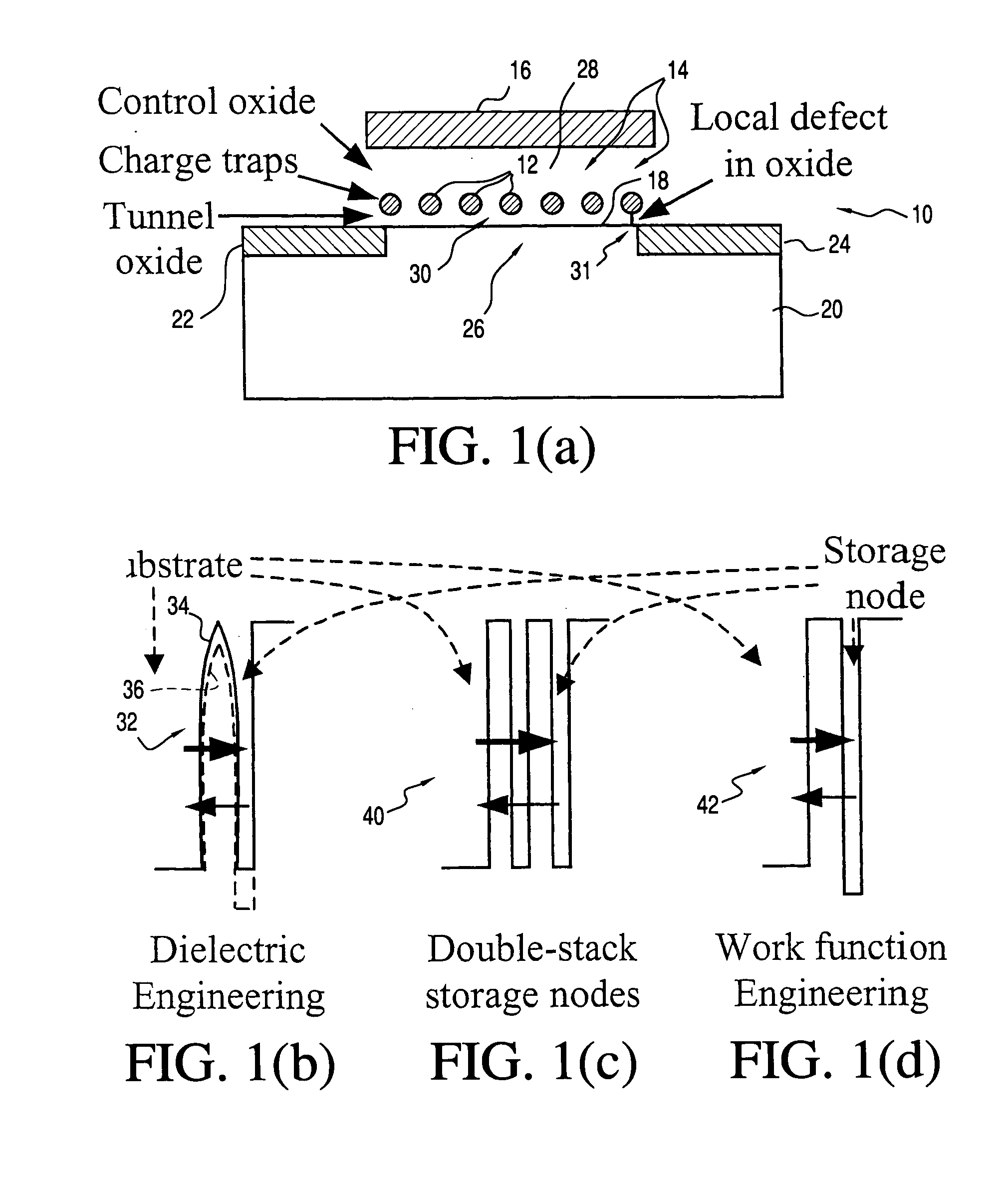
[0042]Turning now to a more detailed description of the invention, FIG. 1(a) illustrates in diagrammatic form a schematic of a memory cell 10 having discrete charge storage elements or nodes 12, which function as charge traps, embedded in an oxide layer 14, or gate dielectric, between a control gate electrode 16 and the surface 18 of a semiconductor substrate 20. Source and drain regions 22 and 24, respectively, are located on the substrate on opposite sides of a channel region 26, which is adjacent the location of the charge storage elements 12. The oxide material between the gate 16 and the charge storage elements 12 is referred to herein as the control oxide 28, while the oxide material between the elements 12 and the surface 18 is referred to as the tunnel oxide 30.

[0043]As illustrated in FIG. 1(a), when stored in discrete traps or nodes, charges are more immune to the leakage caused by localized oxide defects, such as the defect illustrated at 31, thus improving the device rete...


PUM


Abstract

Metal nanocrystal memories are fabricated to include higher density states, stronger coupling with the channel, and better size scalability, than has been available with semiconductor nanocrystal devices. A self-assembled nanocrystal formation process by rapid thermal annealing of ultra thin metal film deposited on top of gate oxide is integrated with NMOSFET to fabricate such devices. Devices with Au, Ag, and Pt nanocrystals working in the F-N tunneling regime, with hot-carrier injection as the programming mechanism, demonstrate retention times up to 106s, and provide 2-bit-per-cell storage capability.

Description

CROSS-REFERENCE TO RELATED APPLICATIONS[0001]This application claims the benefit of Provisional Application No. 60 / 428,906, filed Nov. 26, 2002, the disclosure of which is hereby incorporated herein by reference.GOVERNMENT SPONSORSHIP STATEMENT [0002]This invention was made with Government support from the National Science Foundation (NSF) under Grant No. 9,980,100. The Government has certain rights in the invention.BACKGROUND OF THE INVENTION[0003]The present invention relates, in general, to metal nanocrystals and methods of fabricating the same, and more particularly to semiconductor memory devices incorporating metal nanocrystals to provide a multibit-per-cell storage capability.[0004]Conventional DRAM or Flash memories have been widely employed for many years in a variety of applications. DRAMs allow fast write / erase, but suffer from high power consumption incurred by the constant refresh operations due to their short retention time of less than a few seconds (see B. El-Kareh e...

Claims


Application Information

Patent Timeline
IPC IPC(8): G11C11/34G11C11/56G11C16/04H01L21/28
CPCB82Y10/00G11C11/5671G11C16/0475H01L21/28273G11C16/0491G11C2216/06H01L29/40114
Inventor KAN, EDWIN C.LIU, ZENGTAOLEE, CHUNGHO
Owner CORNELL RES FOUNDATION INC
Why Eureka
Try Eureka