Light-emitting diode packaging process

A technology of light-emitting diodes and packaging technology, which is applied to semiconductor devices, electrical components, circuits, etc., can solve problems such as heat dissipation effects, electroplating process is not environmentally friendly, and differences in the thickness of crystal-bonding adhesives, so as to avoid differences in product quality and reflectivity. Undesirable, Avoid Effects of Plating Procedures

Inactive Publication Date: 2015-02-11
惠州市华阳光电技术有限公司
View PDF7 Cites 3 Cited by
  • Summary
  • Abstract
  • Description
  • Claims
  • Application Information

AI Technical Summary

Problems solved by technology

[0004] Although the above-mentioned method of manufacturing lamp beads has mature technology and strong operability, this method also has certain defects: the light-emitting diode 02 is fixed by spot-coating the crystal-bonding glue 05 on the electroplating layer 04. When the crystal glue 05 is dot-coated on the electroplating layer 04, it is in the form of multi-point accumulation, and the accumulation of each point of the crystal-bonding glue 05 cannot accurately control the amount of dot coating, resulting in differences in the thickness of the crystal-bonding glue 05 at different points , leading to different heat dissipation effects of different light-emitting diodes 02, which in turn causes a large difference in the product quality of different lamp beads, which has a greater impact on the consistency of the quality of different lamp beads
[0005] In addition, the electroplating process is not environmentally friendly, the reflectivity of the electroplating layer is not ideal, and it has an impact on heat dissipation. At the same time, the electroplating layer also has the risk of being oxidized and vulcanized, and the cost is high

Method used


Image

  • Light-emitting diode packaging process
  • Light-emitting diode packaging process
  • Light-emitting diode packaging process

Examples


Embodiment Construction

[0027] The invention provides a packaging process of light-emitting diodes, which can improve the quality consistency of different lamp beads.

[0028] The following will clearly and completely describe the technical solutions in the embodiments of the present invention with reference to the accompanying drawings in the embodiments of the present invention. Obviously, the described embodiments are only some, not all, embodiments of the present invention. Based on the embodiments of the present invention, all other embodiments obtained by persons of ordinary skill in the art without making creative efforts belong to the protection scope of the present invention.

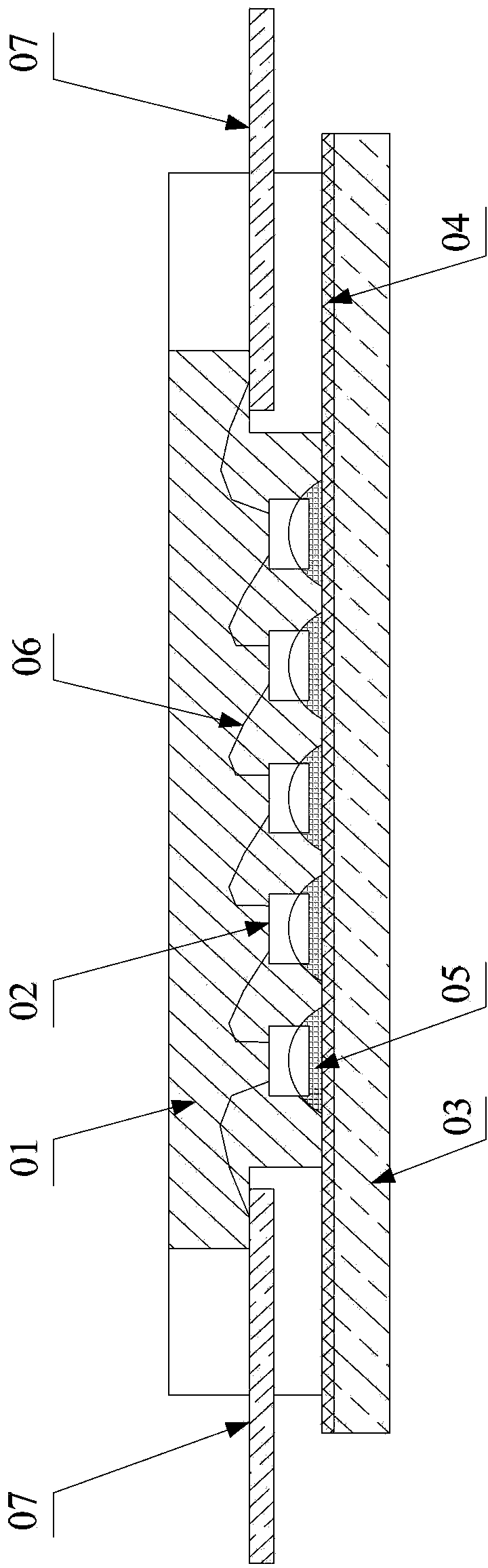
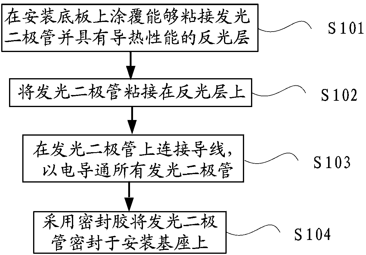
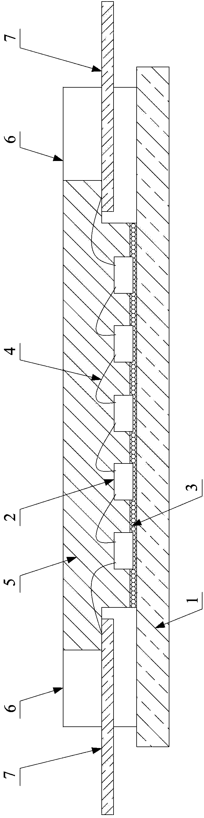
[0029] Such as figure 2 and image 3 As shown, the packaging process of the light emitting diode provided by the embodiment of the present invention includes the following steps:

[0030] S101, coating the light-reflecting layer 3 capable of bonding the light-emitting diode 2 and having thermal conductivity on the ...


PUM


Abstract

The invention provides a light-emitting diode packaging process. The method comprises the following steps that a light-reflecting layer which can be stuck to a light-emitting diode and has heat conductivity is coated on a mounting bottom plate; the light-emitting diode is stuck to the light-reflecting layer; a lead is connected to the light-emitting diode, so that the light-emitting diode is electrified; the light-emitting diode is sealed on the mounting bottom plate by a sealing adhesive. According to the light-emitting diode provided by the invention, an electroplated layer and a crystal solidifying adhesive are substituted by the light-reflecting layer; due to the fact that the top surface and the bottom surface of the light-reflecting layer are planes and are coating layers which are in an integral form, and the coating thickness and the uniformity of the top surface and the bottom surface are more precisely controlled than the crystal solidifying adhesive which are arranged at multiple points and are stacked, the radiating effect of a plurality of light-emitting diodes stuck to different positions and having the same thickness on the light-reflecting layer are consistent by precisely controlling the thickness of the light-reflecting layer, the quality difference of different lamp beads is reduced even avoided, and the quality consistency of different lamp beads is further improved.

Description

technical field [0001] The invention relates to the technical field of LED lighting equipment, and more specifically, to a packaging process of light emitting diodes. Background technique [0002] With the continuous development of semiconductor lighting technology, more and more LED (English Light-Emitting Diode abbreviation, light-emitting diode) lights have entered various lighting fields. [0003] The light-emitting part of an LED lamp is commonly called a lamp bead, that is, a part in which a plurality of light-emitting diodes 02 are packaged into one body with a transparent sealant 01. The manufacturing process of the lamp bead, that is, the packaging process of the light-emitting diode is: stamping the bottom plate 03; electroplating and injection on the bottom plate 03 to form an electroplating layer 04, which can reflect light and illuminate the light-emitting diode 02 The light on the electroplating layer 04 is reflected to improve the light output rate of the lam...

Claims


Application Information

Patent Timeline
Patent Type & Authority Applications(China)
IPC IPC(8): H01L25/075H01L33/62H01L33/64
CPCH01L2224/45144H01L2224/48091H01L2224/48137H01L2224/73265H01L2924/00014H01L2924/00
Inventor 刘华基王峰曾昌景
Owner 惠州市华阳光电技术有限公司
Why Eureka
Try Eureka