

Diode photoelectricity test method
A photoelectric test and diode technology, applied in the field of diodes, can solve the problems of easy burning of test probes, affecting test accuracy, increasing production costs, etc., to achieve the effects of reducing area, saving production costs and improving accuracy
Active Publication Date: 2015-02-18
HC SEMITEK SUZHOU
View PDF5 Cites 16 Cited by
- Summary
- Abstract
- Description
- Claims
- Application Information
AI Technical Summary
Problems solved by technology
[0006] In order to solve the problem in the prior art that the test probe is easy to burn during the test, which increases the production cost, and the test probe will block part of the light-emitting area of the chip and affect the accuracy of the test, the embodiment of the present invention provides a photoelectric sensor for a diode. testing method
Method used
View moreImage
Smart ImageViewing Examples

Examples
Embodiment
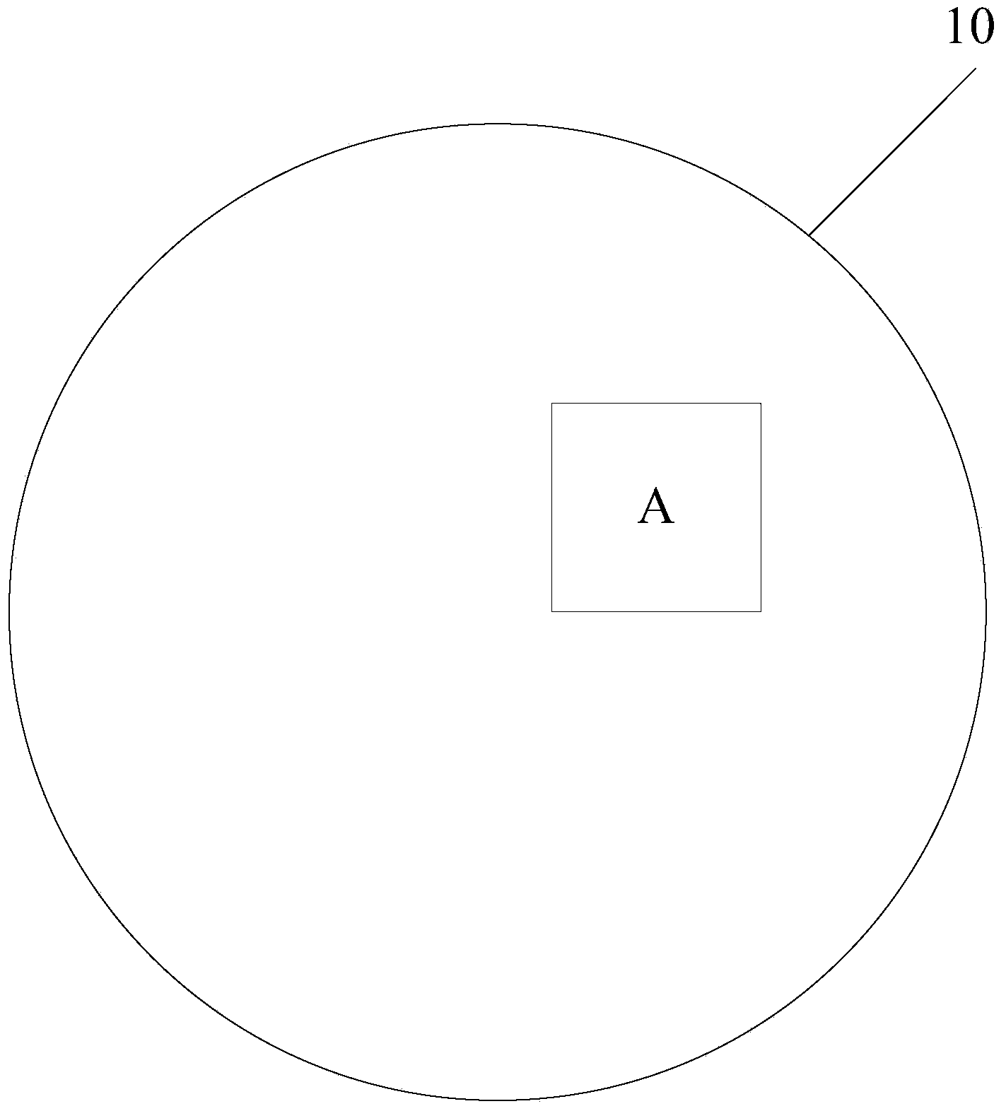
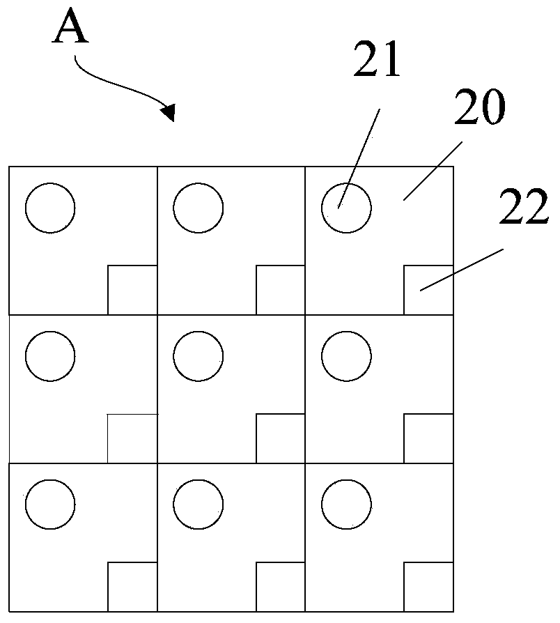
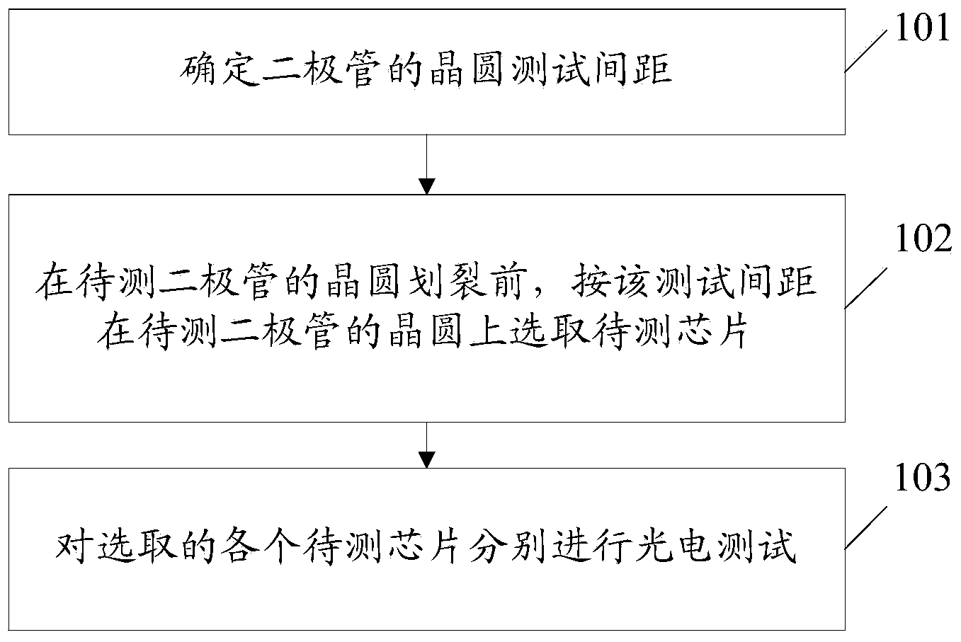
[0039] An embodiment of the present invention provides a photoelectric test method for diodes, which is suitable for wafer testing of diodes, see figure 2 and image 3 , the method includes:
[0040] Step 101: Determine the wafer testing pitch of the diode.
[0041] According to production needs, determine the wafer test pitch of the diode.
Login to View More PUM
 Abstract
The invention belongs to the field of diodes and discloses a diode photoelectricity test method. The method includes: determining a diode wafer test distance; selecting to-be-tested chips on a wafer of a to-be-tested diode according to the test distance before the wafer of the to-be-tested diode is scratched; subjecting the selected to-be-tested chips to photoelectricity test respectively. The step of subjecting the selected to-be-tested chips to photoelectricity test respectively includes: connecting a first test probe into a P-electrode of the current to-be-tested chip; connecting a second test probe into an N-electrode of a first chip, wherein the first chip and the current to-be-tested chip are both positioned on the wafer of the to-be-tested diode; charging rated current or rated voltage to the first test probe and the second test probe; detecting photoelectric parameters of the to-be-tested chips by measurement equipment.
Description
technical field [0001] The invention relates to the field of diodes, in particular to a photoelectric testing method for diodes. Background technique [0002] With the wide application of gallium nitride-based compound light-emitting diodes (English: Lighting Emitting Diode, referred to as: LED) in the field of display and lighting, the demand for LEDs has shown a geometric progression in recent years, which has a negative impact on the production efficiency of LEDs. and production quality put forward higher requirements. [0003] In the manufacturing process of diodes such as LEDs, it is necessary to conduct photoelectric tests on the wafers of the diodes. During the test, it is necessary to use test probes to pierce the N and P electrodes of the chip on the wafer at the same time to perform a complete photoelectric performance test. The chip needs to pass current multiple times. [0004] In the process of realizing the present invention, the inventor finds that there are...
Claims
Login to View More Application Information
Patent Timeline
 IPC IPC(8): G01R31/26
Inventor陈建南周武
OwnerHC SEMITEK SUZHOU