

Electronic system with a composite substrate
A technology for electronic components and electronic devices, applied in circuits, printed circuits, electrical components, etc., to solve problems such as inability to conduct heat
- Summary
- Abstract
- Description
- Claims
- Application Information
AI Technical Summary
Problems solved by technology
Method used
Image

Examples
Embodiment 1
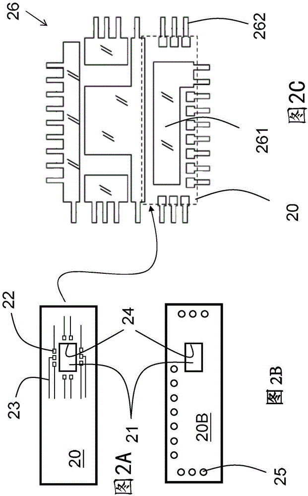
[0059] Such as Figure 2A The display circuit board 20 has a rectangular opening 21 , and a group of metal pads 22 surround four edges 24 of the rectangular opening 21 . The metal pad 22 is a part of the circuit on the circuit board 20 , and the metal pad 22 is electrically coupled to the circuit (not shown) on the circuit board 20 via the metal wire 23 .
[0060] Such as Figure 2B As shown, a set of bottom metal contacts 25 are disposed on the bottom surface 20B of the circuit board 20 , and the metal contacts 25 are subsequently electrically coupled to corresponding metal pins 262 on the circuit board 20 .
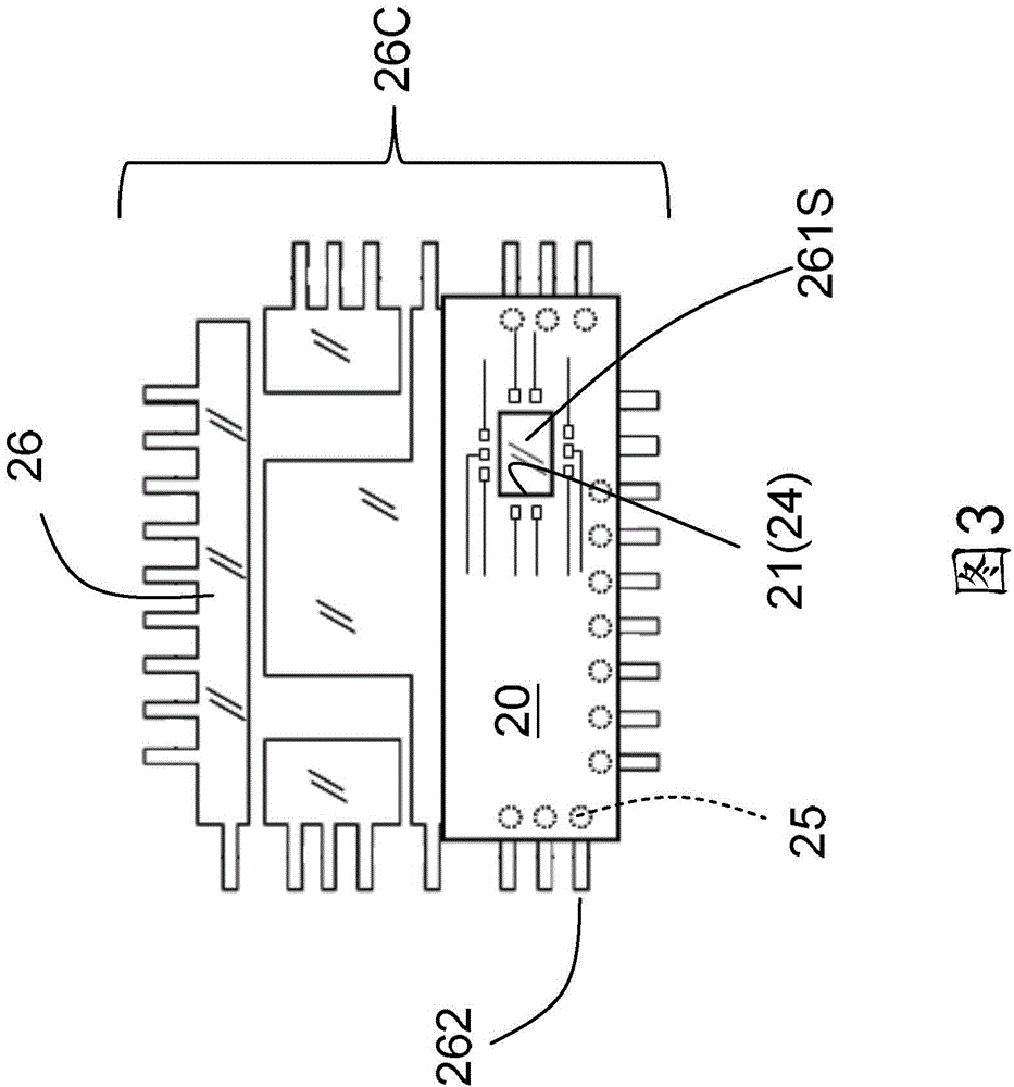
[0061] Such as Figure 2C As shown, a metal frame 26 has several large pieces of metal 261, which can carry high-heating electronic components; the metal frame 26 also has a set of peripheral metal feet 262 distributed around the metal frame 26, followed by packaging After packaging, the peripheral metal pins 262 serve as output / input pins of the electronic system. ...
Embodiment 2
[0068] Such as Figure 5A As shown, the edge of the circuit board 203 has a U-shaped opening 213 , and a group of metal pads 223 are disposed beside three edges 243 of the U-shaped opening 213 . The metal pad 223 is a part of the circuit on the circuit board 203 , and the metal pad 223 is electrically coupled to the circuit (not shown) on the circuit board 203 through the metal wire 233 . A group of metal contacts 253 are disposed on the bottom surface of the circuit board 203 as the input and output contacts of the circuit on the circuit board 203 .
[0069] Such as Figure 5B As shown, the metal frame 26 has a plurality of large pieces of metal 261, and the large pieces of metal 261 are suitable for carrying high-heat-generating electronic components such as chips; a group of peripheral metal feet 262 are placed on the periphery of the metal frame 26 as a follow-up entire electronic system The output and output contacts. Subsequently, the circuit board 203 will be placed ...
Embodiment 3
[0073] Such as Figure 6A As shown, the edge of the circuit board 202 has an L-shaped opening 212 , and a set of metal pads 222 are disposed beside two edges 242 of the L-shaped opening 212 . The metal pad 222 is a part of the circuit on the circuit board 202 , and the metal pad 222 is electrically coupled to the circuit on the circuit board 202 through the metal wire 232 . A group of metal contacts 252 are disposed on the bottom surface of the circuit board 202 as the input and output contacts of the circuit on the circuit board 202 .
[0074] Such as Figure 6B As shown, the basic idea of this embodiment is the same as that of Embodiment 1-2, the only difference is that the shape of the opening of the circuit board is different. Figure 6A The display circuit board 202 has an L-shaped opening 212 , and the chip 302 is disposed on the metal surface 261S exposed by the opening 212 . The circuits in the chip 302 are electrically coupled to the circuits on the circuit board...
PUM
 Abstract
Description
Claims
Application Information