Electronic system with a composite substrate

一种电子系统、复合基材的技术,应用在电路、印刷电路、电气元件等方向,能够解决传导等问题

Inactive Publication Date: 2011-08-17
CYNTEC
View PDF6 Cites 2 Cited by
  • Summary
  • Abstract
  • Description
  • Claims
  • Application Information

AI Technical Summary

Problems solved by technology

[0003] One of the disadvantages of the aforementioned electronic system is that the system circuit board 120 is not a good heat sink, and cannot effectively transfer the heat generated by the electronic components 120, 130, 140, 150, 160, and 170 mounted on it to the bottom. The copper substrate 110 for heat dissipation

Method used


Image

  • Electronic system with a composite substrate
  • Electronic system with a composite substrate
  • Electronic system with a composite substrate

Examples


Embodiment 1

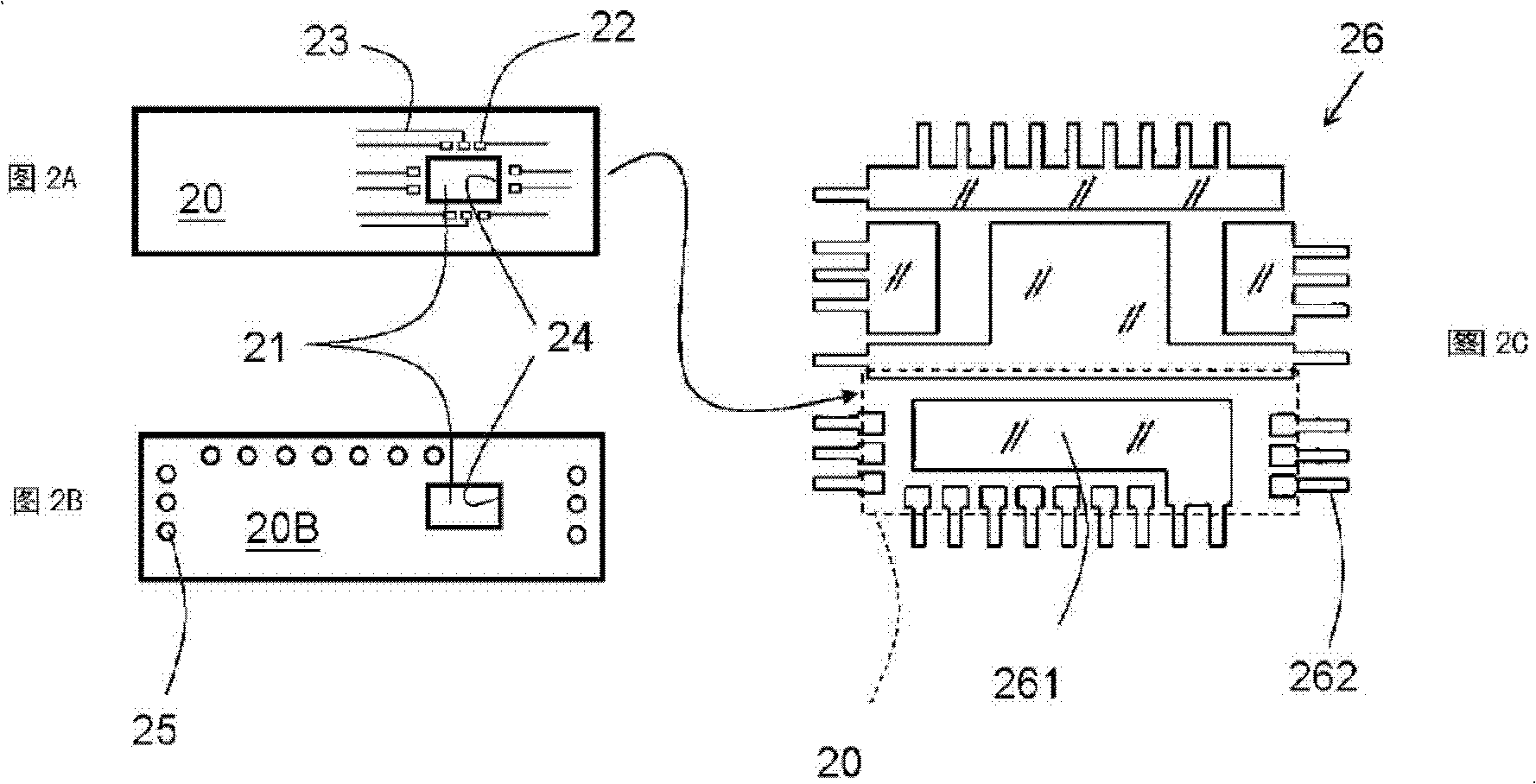
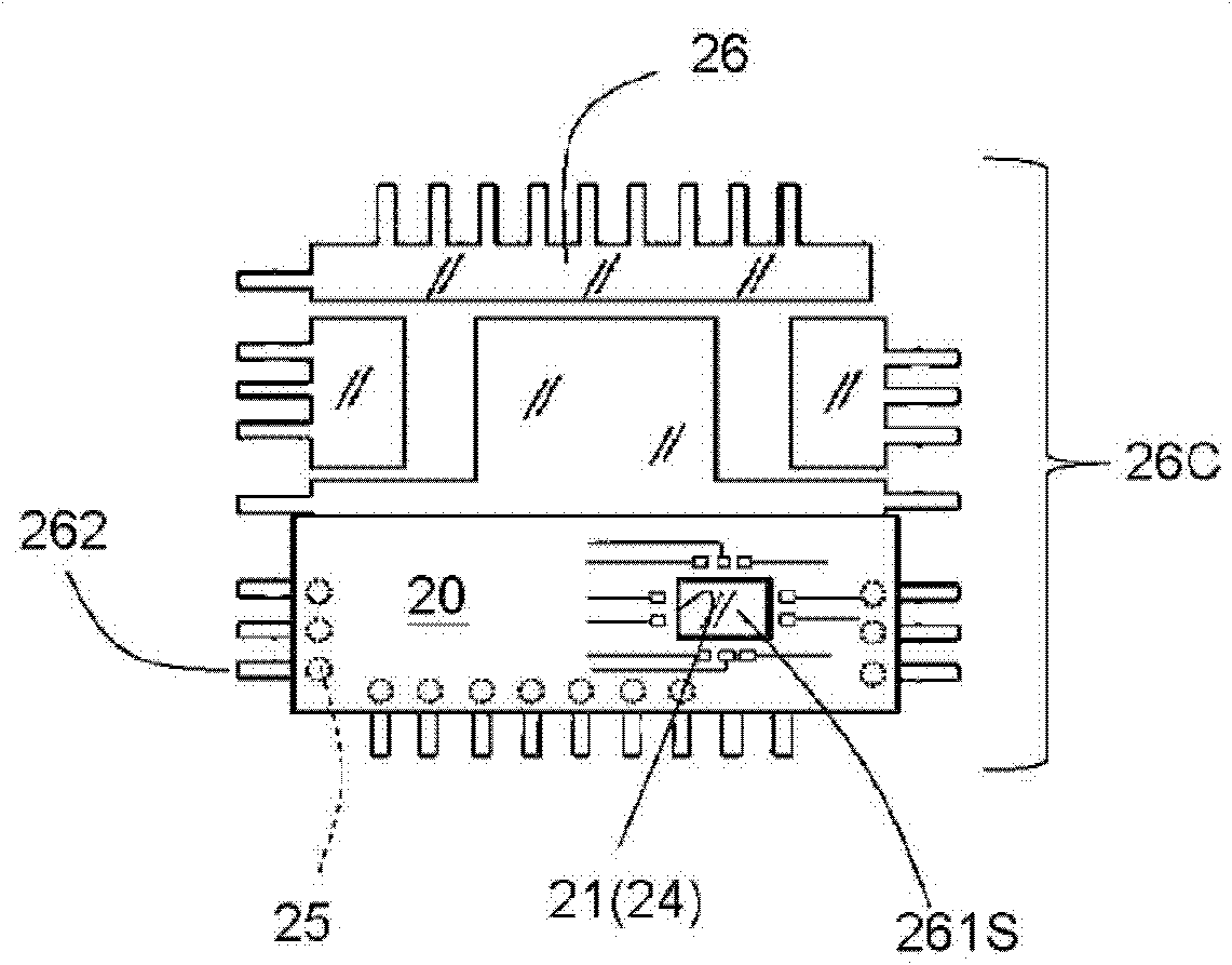
[0036] like Figure 2A The display circuit board 20 has a rectangular opening 21 , and a group of metal pads 22 surround four edges 24 of the rectangular opening 21 . The metal pad 22 is a part of the circuit on the circuit board 20 , and the metal pad 22 is electrically coupled to the circuit (not shown) on the circuit board 20 via the metal wire 23 .

[0037] like Figure 2B As shown, a set of bottom metal contacts 25 are disposed on the bottom surface 20B of the circuit board 20 , and the metal contacts 25 are subsequently electrically coupled to corresponding metal pins 262 on the circuit board 20 .

[0038] like Figure 2C As shown, a metal frame 26 has several large pieces of metal 261, which can carry high-heating electronic components; the metal frame 26 has a set of peripheral metal feet 262 distributed around the metal frame 26, followed by encapsulation colloid After packaging, the peripheral metal pins 262 serve as output / input pins of the electronic system. Th...

Embodiment 2

[0045] like Figure 5AAs shown, the edge of the circuit board 203 has a U-shaped opening 213 , and a group of metal pads 223 are disposed beside three edges 243 of the U-shaped opening 213 . The metal pad 223 is a part of the circuit on the circuit board 203 , and the metal pad 223 is electrically coupled to the circuit (not shown) on the circuit board 203 through the metal wire 233 . A group of metal contacts 253 are disposed on the bottom surface of the circuit board 203 as the input and output contacts of the circuit on the circuit board 203 .

[0046] like Figure 5B As shown, the metal frame 26 has a plurality of large pieces of metal 261, and the large pieces of metal 261 are suitable for carrying high heat generating electronic components such as chips; The input and output contacts of the electronic system. Subsequently, the circuit board 203 will be placed on the metal frame 26 .

[0047] like Figure 5C as shown, Figure 5A The circuit board 203 shown is housed...

Embodiment 3

[0050] like Figure 6A As shown, the edge of the circuit board 202 has an L-shaped opening 212 , and a set of metal pads 222 are disposed beside two edges 242 of the L-shaped opening 212 . The metal pad 222 is a part of the circuit on the circuit board 202 , and the metal pad 222 is electrically coupled to the circuit on the circuit board 202 through the metal wire 232 . A group of metal contacts 252 are disposed on the bottom surface of the circuit board 202 as the I / O contacts of the circuit on the circuit board 202 .

[0051] like Figure 6B As shown, the basic idea of ​​this embodiment is the same as that of Embodiment 1-2, the only difference is that the shape of the opening of the circuit board is different. Figure 6A The display circuit board 202 has an L-shaped opening 212 , and the chip 302 is disposed on the metal surface 261S exposed by the opening 212 . The circuits in the chip 302 are electrically coupled to the circuits on the circuit board 202 via metal wire...


PUM


Abstract

A composite substrate made of a circuit board mounted on a lead frame is used for an electronic system package. High heat generated electronic components are adapted to mount on the lead frame and relatively low heat generated electronic components are adapted to mount on the circuit board. Metal lines are used for electrical coupling between the circuitry of the IC chip and the circuit board. An electronic system with the composite substrate gains both advantages-good circuitry arrangement capability from the circuit board and good heat distribution from the lead frame.

Description

technical field [0001] The present invention relates to an electronic system; in particular, it relates to the packaging of the electronic system with a composite base material, and the composite base material is a composite base material composed of a circuit board and a metal frame (lead frame). Background technique [0002] like figure 1 As shown, U.S. Patent No. 6,212,086 disclosed a DC-to-DC converter system (DC-to-DC converter system) on April 03, 2001, which includes a copper substrate 110 to provide uniform heat dissipation at the bottom of the system , also includes the circuit board 120 placed on the copper substrate 110, the electronic components include the main transformer 130, output inductor 140, synchronous rectifier 150, output capacitor 160, and input capacitor 170, these components are placed in the system circuit plate 120 above. A separate output connector is on the right side of the system circuit board 120 and is coupled to the system circuit board 1...

Claims


Application Information

Patent Timeline
Patent Type & Authority Applications(China)
IPC IPC(8): H01L23/495H01L23/498
CPCH01L2224/49175H01L2924/0002H05K3/0061H05K2203/1327H01L23/49541H05K2201/10924H05K7/1432H02M3/00H01L23/13H05K1/021H01L23/49531H01L2924/30107H01L2924/13091H01L2924/13055H01L2924/1305H02M3/003H05K7/14322H01L2924/00
Inventor 李翰祥施坤宏李正人
Owner CYNTEC
Why Eureka
Try Eureka