Apparatus and method for fabricating semiconductor chip package with film attached on

A technology for chip packaging and manufacturing devices, applied in semiconductor devices, semiconductor/solid-state device components, electric solid-state devices, etc., can solve the problems of low luminous quality and yield of LED packaging, unusable sealing resin, and low luminous efficiency, etc. Achieve the effect of improving production performance, reducing usage, and low calorific value

Inactive Publication Date: 2015-02-25
人科机械有限公司
View PDF8 Cites 3 Cited by
  • Summary
  • Abstract
  • Description
  • Claims
  • Application Information

AI Technical Summary

Problems solved by technology

[0003] However, in this type of LED package, it is difficult to precisely adjust the thickness of the sealing resin layer mixed with the phosphor and the mixing ratio of the phosphor, resulting in low luminous quality and yield, high heat generation, and low luminous efficiency of the LED package.
[0004] In addition, during long-term storage, the sealing resin hardens and cannot be used, resulting in a problem of increased cost

Method used


Image

  • Apparatus and method for fabricating semiconductor chip package with film attached on
  • Apparatus and method for fabricating semiconductor chip package with film attached on
  • Apparatus and method for fabricating semiconductor chip package with film attached on

Examples


Embodiment Construction

[0069] The manufacturing equipment and manufacturing method of the film-bonded semiconductor chip chip package will be described in detail according to the implementation of the invention with reference to the attached drawings below. The terms (terminology) used in this specification are used to properly express the implementation of this invention, and have different effects depending on the user or the user's intention or language habits in the field to which this invention belongs. Therefore, the definitions of these terms can only be understood by understanding the contents of this specification as a whole.

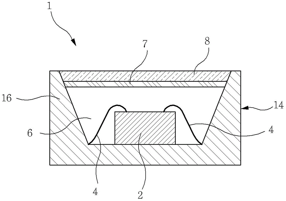
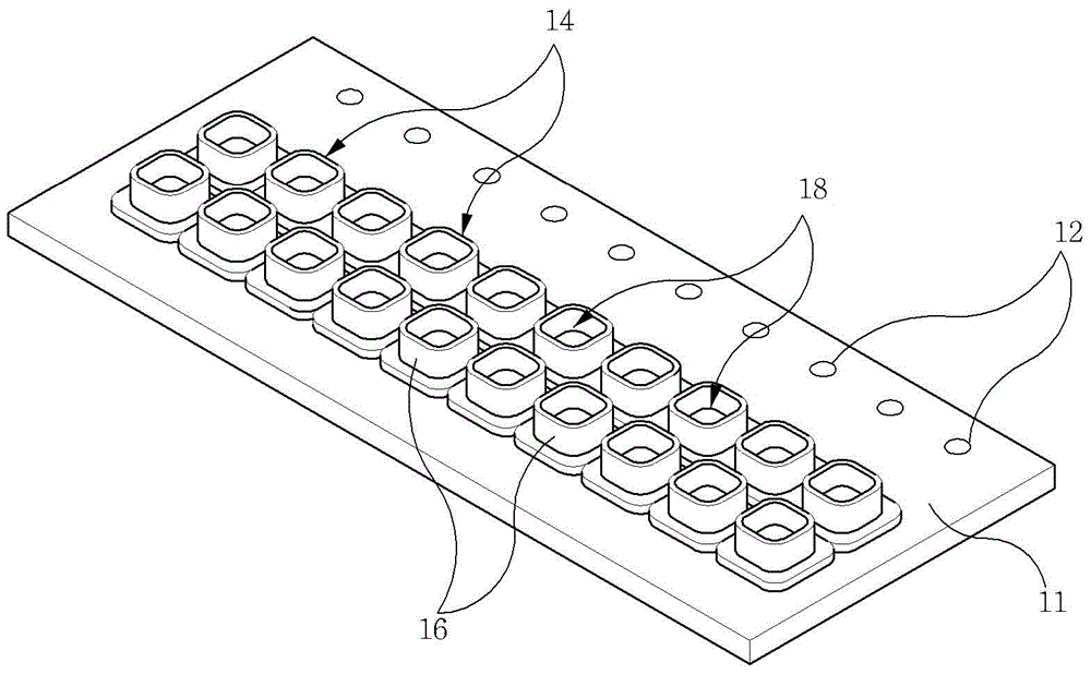
[0070] First of all, use the semiconductor chip chip package manufacturing equipment of this invention to manufacture a kind of semiconductor chip chip, as an example figure 1 It is a one-sided view showing that the fluorescent film is attached to the LED package, figure 2 It is an instruction diagram showing a form in which a lead frame (lead frame) used for manuf...


PUM


Abstract

The invention relates to an apparatus and a method for fabricating a semiconductor chip package with a film attached on. In particular, the invention provides an LED package with a fluorescent film attached on, an apparatus for fabricating the semiconductor chip package with a film attached on and a method for fabricating the semiconductor chip package. The apparatus comprises a lead frame loading unit for loading lead frames sequentially, resin dispensing units for sealing, a thin film stage, a thin film attaching unit and a lead frame unloading unit. The resin dispensing units are used for injecting sealing resin on the lead wire frameworks and formed on chip receiving parts of the lead frames in a sealed manner. In a thin film stage, fluorescent film slices are moved to a pickup position in order. Via the thin film attaching unit, after being absorbed, the fluorescent film slices in a material receiving position are attached to the resin for sealing of the lead frames. After the lead frames passing through the thin film are unloaded, the lead frame unloading unit recovers the action.

Description

technical field [0001] The present invention relates to a semiconductor chip package manufacturing device and a manufacturing method for continuously manufacturing a semiconductor chip package such as a fluorescent film-coated LED package. Background technique [0002] LED packaging used for indicators of electronic equipment, backlight units of LCD screens, lighting devices, etc., generally a semiconductor chip chip LED (light emitting diode) is installed behind the lead frame to protect the LED and click The connecting portion is sealed with a translucent resin. The sealing resin is, for example, silicone resin (silicone), and phosphor powder is mixed in the sealing resin in order to increase the luminance when emitting light. [0003] However, it is difficult to precisely adjust the thickness of the sealing resin layer mixed with the phosphor and the mixing ratio of the phosphor in this type of LED package, resulting in low luminous quality and yield, high heat generatio...

Claims


Application Information

Patent Timeline
Patent Type & Authority Applications(China)
IPC IPC(8): H01L33/00H01L33/48
CPCH01L33/00H01L33/48H01L33/62H01L2224/45139H01L2224/48091H01L2924/00014H01L2924/00H01L23/28H01L33/52
Inventor 金准燮河商宽
Owner 人科机械有限公司
Why Eureka
Try Eureka