N-type silicon solar cell, its preparation method and aluminum evaporation and diffusion device
A technology of solar cells and n-type silicon, which is applied in circuits, photovoltaic power generation, electrical components, etc., can solve the problems of many impurities, different layer thicknesses, and low cell efficiency, and achieve economical and simple devices, scientific preparation methods, and improved uniformity. sexual effect
- Summary
- Abstract
- Description
- Claims
- Application Information
AI Technical Summary
Problems solved by technology
Method used
Image
Examples
Embodiment 1
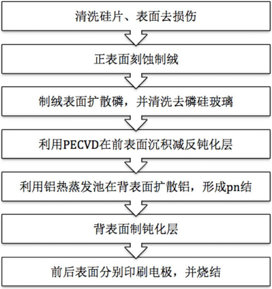
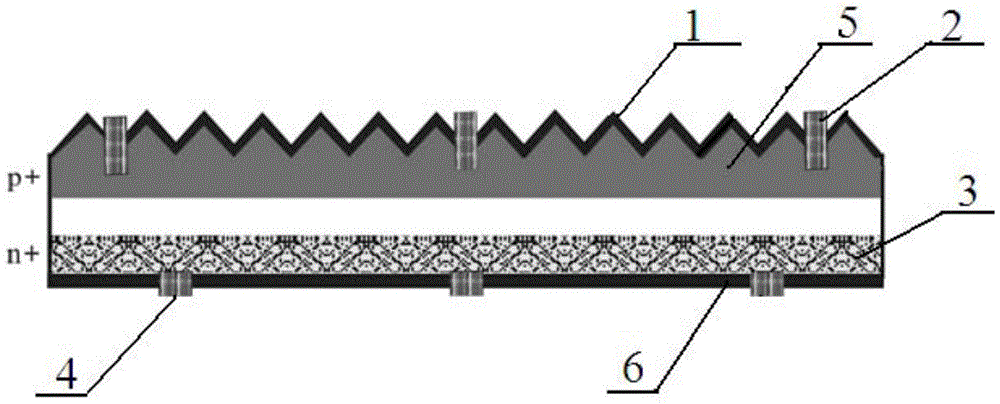
[0053] figure 1 It is the flow chart of the preparation method of the n-type silicon front junction solar cell of embodiment 1; Image 6 It is a schematic structural diagram of an aluminum evaporation and diffusion device used to prepare an n-type silicon solar cell in the present invention; image 3 Schematic diagram of the structure of the n-type silicon front-junction solar cell prepared in Example 1; Figure 7 It is a schematic diagram of the array carrier structure of the silicon wafer and the mask plate.
[0054] This embodiment relates to a method for preparing an n-type silicon front-junction solar cell. In this method, an aluminum film is deposited on a silicon wafer by thermal evaporation, and the silicon wafer is heated to realize aluminum diffusion to form a pn junction, and an n-type silicon front-junction solar cell is obtained. Battery.
[0055] In order to deposit an aluminum film on a silicon wafer by thermal evaporation, this embodiment uses an aluminum ev...
Embodiment 2
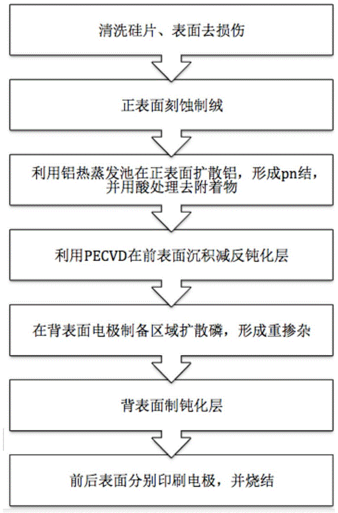
[0075] figure 2 It is the flow chart of the preparation method of the n-type silicon back-junction solar cell of embodiment 2; Figure 4 Schematic diagram of the structure of the n-type silicon back-junction solar cell prepared in Example 2; Figure 8 is a schematic diagram of the structure of diffusion mask plate 1;
[0076] In this embodiment, the same aluminum evaporation and diffusion device used for preparing n-type silicon solar cells as in Embodiment 1 is used.
[0077] The preparation method of n-type silicon back-junction solar cell in this embodiment is as follows figure 2 shown, including the following steps:
[0078] (1) cleaning, and the step of polishing n-type silicon chip is identical with embodiment 1;
[0079] (2) Etching texture on the front surface of the silicon by chemical method. The texture structure is pyramid-shaped, with a tower height of 2-3 microns;
[0080] (3) Diffusion of phosphorus in the front field on the surface after texturing to fo...
Embodiment 3
[0087] Figure 5 Schematic diagram of the structure of the n-type silicon back-junction solar cell prepared in Example 3; Figure 9 It is a schematic diagram of the structure of diffusion mask plate 2.
[0088] In this embodiment, the same aluminum evaporation and diffusion device used for preparing n-type silicon solar cells as in Embodiment 1 is used.
[0089] The preparation method of the interdigitated n-type monocrystalline silicon solar cell with n-type back junction and back contact in this embodiment is as follows:
[0090] (1) cleaning, and the method of polishing n-type silicon chip is identical with embodiment 1;
[0091] (2) Utilize the chemical method to etch the texture on the front surface of the silicon, the texture structure is pyramid-shaped, and the height of the tower is 2-3 microns;
[0092] (3) Diffusion of phosphorus in the front field on the front surface after texturing to form n + Area;
[0093] (4) Utilize PECVD or ALD to deposit SiNx anti-refle...
PUM
 Abstract
Description
Claims
Application Information


