Reflection electrode structure, LED device and preparation method

A technology of LED devices and reflective electrodes, applied in electrical components, semiconductor devices, circuits, etc., can solve problems such as brightness reduction

Active Publication Date: 2015-03-04
XIANGNENG HUALEI OPTOELECTRONICS
View PDF5 Cites 10 Cited by
  • Summary
  • Abstract
  • Description
  • Claims
  • Application Information

AI Technical Summary

Problems solved by technology

[0004] The purpose of the present invention is to overcome the above disadvantages and provide a reflective electrode structure to solve the problem that the brightness of the existing LED chip is reduced due to the light absorption of the electrode

Method used


Image

  • Reflection electrode structure, LED device and preparation method
  • Reflection electrode structure, LED device and preparation method
  • Reflection electrode structure, LED device and preparation method

Examples


Embodiment 1

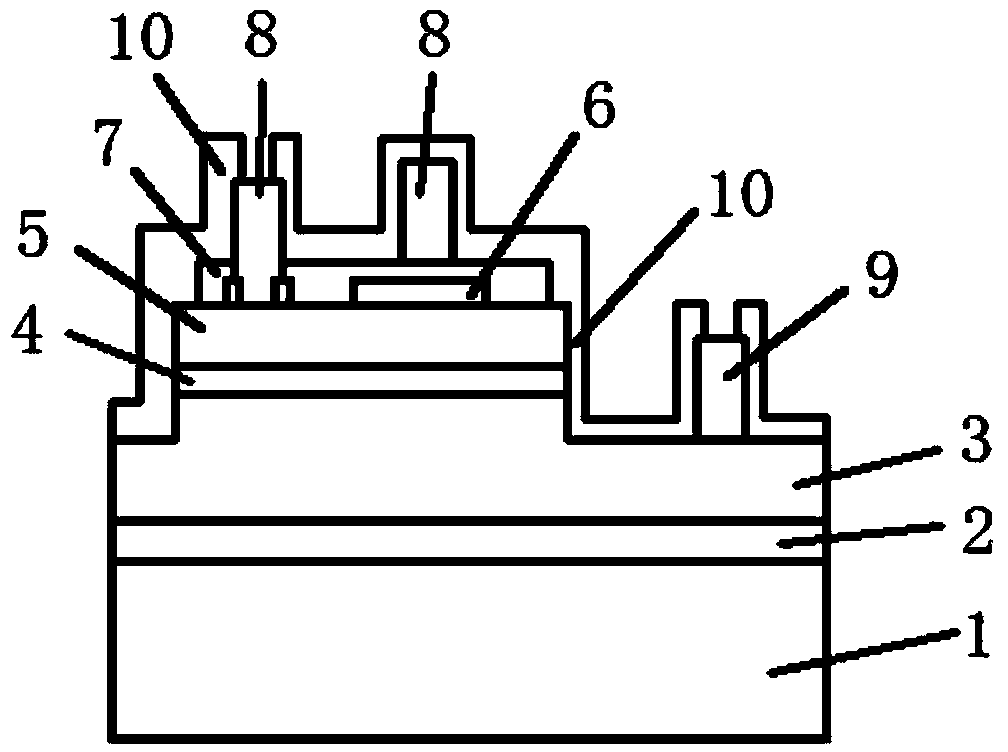
[0072] The reflective electrode structure of this embodiment is disposed on the nitride semiconductor layer and includes: a reflective portion and an electrode portion, the electrode portion is located on the reflective portion, wherein the reflective portion is made of the nitride semiconductor The surface layer of the layer is composed of a first Ni layer and an Al layer sequentially arranged outward; the electrode part is composed of a Cr layer, a second Ni layer and an Au layer sequentially arranged outward from the Al layer of the reflective part, or composed of all The Al layer of the reflective part is composed of a Cr layer, a Pt layer, and an Au layer that are sequentially arranged outward, or a second Ni layer, a Pt layer, and an Au layer are sequentially arranged outward of the Al layer of the reflective part, or The Al layer of the reflective part is composed of Ti layer, Pt layer and Au layer arranged in sequence outwards, or Ti layer, Pt layer, Ti layer, Pt layer, ...

Embodiment 2

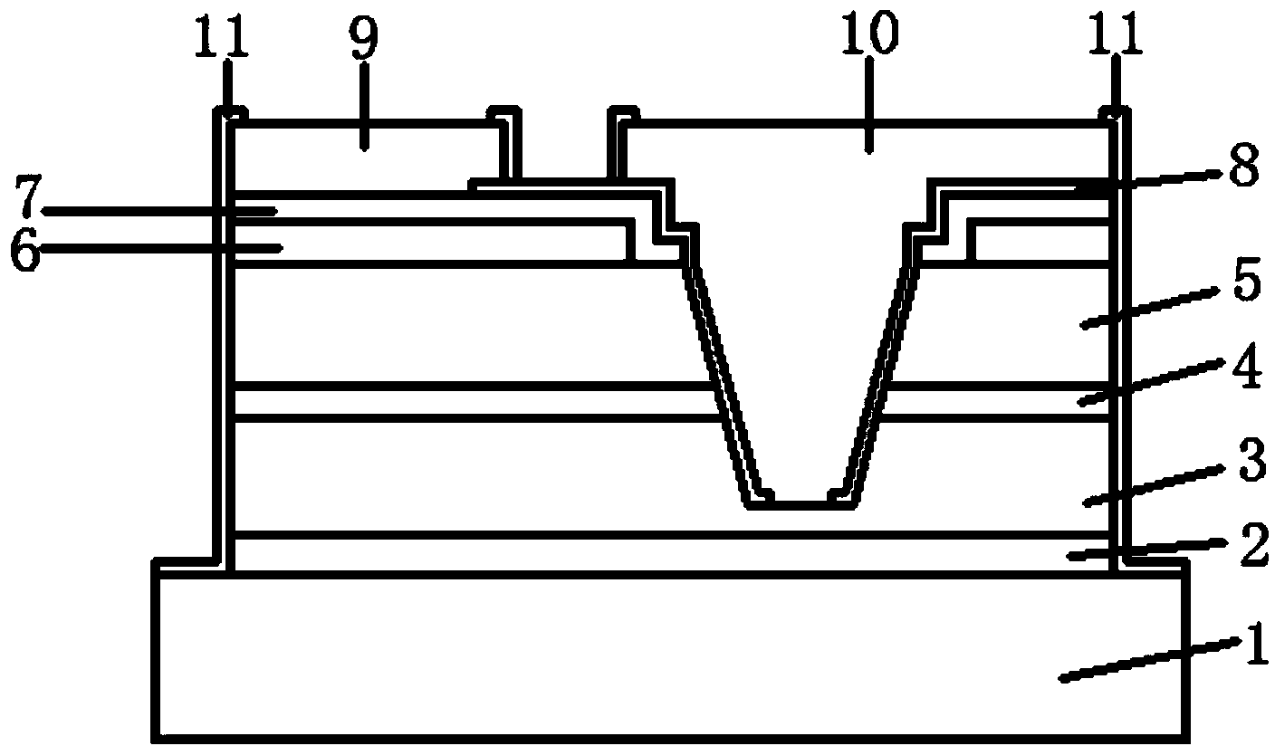
[0081] The reflective electrode structure of this embodiment is disposed on the nitride semiconductor layer and includes: a reflective portion and an electrode portion, the electrode portion is located on the reflective portion, wherein the reflective portion is made of the nitride semiconductor The surface layer of the layer is composed of a first Ni layer and an Al layer sequentially arranged outward; the electrode part is composed of a Cr layer, a second Ni layer and an Au layer sequentially arranged outward from the Al layer of the reflective part, or composed of all The Al layer of the reflective part is composed of a Cr layer, a Pt layer, and an Au layer that are sequentially arranged outward, or a second Ni layer, a Pt layer, and an Au layer are sequentially arranged outward of the Al layer of the reflective part, or The Al layer of the reflective part is composed of Ti layer, Pt layer and Au layer arranged in sequence outwards, or Ti layer, Pt layer, Ti layer, Pt layer, ...

Embodiment 3

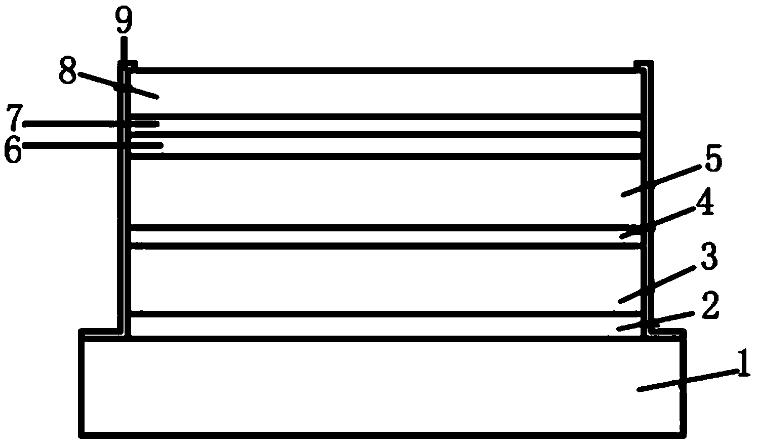
[0090] The reflective electrode structure of this embodiment is disposed on the nitride semiconductor layer and includes: a reflective portion and an electrode portion, the electrode portion is located on the reflective portion, wherein the reflective portion is made of the nitride semiconductor The surface layer of the layer is composed of a first Ni layer and an Al layer sequentially arranged outward; the electrode part is composed of a Cr layer, a second Ni layer and an Au layer sequentially arranged outward from the Al layer of the reflective part, or composed of all The Al layer of the reflective part is composed of a Cr layer, a Pt layer, and an Au layer that are sequentially arranged outward, or a second Ni layer, a Pt layer, and an Au layer are sequentially arranged outward of the Al layer of the reflective part, or The Al layer of the reflective part is composed of Ti layer, Pt layer and Au layer arranged in sequence outwards, or Ti layer, Pt layer, Ti layer, Pt layer, ...


PUM

PropertyMeasurementUnit
thicknessaaaaaaaaaa
thicknessaaaaaaaaaa
thicknessaaaaaaaaaa

Abstract

The application discloses a reflection electrode structure which is arranged on a nitride semiconductor layer. The reflection electrode structure comprises a reflection part and an electrode part which is arranged on the reflection part. The reflection part is composed of a first Ni layer and an Al layer which are outwardly arranged in turn from the surface of the nitride semiconductor layer. The electrode part is composed of a Cr layer, a second Ni layer and an Au layer which are outwardly arranged in turn from the Al layer of the reflection part, or is composed of the Cr layer, a Pt layer and the Au layer which are outwardly arranged in turn from the Al layer of the reflection part, or is composed of the second Ni layer, the Pt layer and the Au layer which are outwardly arranged in turn from the Al layer of the reflection part, or is composed of a Ti layer, the Pt layer and the Au layer which are outwardly arranged in turn from the Al layer of the reflection part, or is composed of the Ti layer, the Pt layer, the Ti layer, the Pt layer, the Ti layer, the Pt layer and the Au layer which are outwardly arranged in turn from the Al layer of the reflection part. Light emergent efficiency of the electrode can be enhanced and operation current can be reduced.

Description

Technical field [0001] The invention belongs to the technical field of semiconductors, relates to a reflective electrode structure, and also relates to an LED device and a preparation method. Background technique [0002] The LED chip usually includes a semiconductor light-emitting structure that generates light radiation after being energized, and an electrode that connects the semiconductor structure to an external power source. A gallium nitride-based light-emitting diode is a light-emitting device that converts electrical energy into light energy with high efficiency. The electrode materials are mostly titanium aluminum and titanium gold. The patent document with publication number CN103985805A discloses a light-emitting device whose wire electrode adopts relatively low-priced titanium aluminum material, and a titanium layer and a thick aluminum layer are successively evaporated , By appropriately increasing the thickness of the metal layer of the wire electrode, the failure ...

Claims


Application Information

Patent Timeline
Patent Type & Authority Applications(China)
IPC IPC(8): H01L33/40H01L33/00
CPCH01L33/0075H01L33/405H01L33/42H01L2933/0016
Inventor 许顺成梁智勇蔡炳杰
Owner XIANGNENG HUALEI OPTOELECTRONICS
Why Eureka
Try Eureka