Organic electroluminescence device and preparation method thereof

An electroluminescent device and an organic light-emitting layer technology, which is applied in the direction of organic light-emitting devices, organic light-emitting device structures, circuits, etc., can solve problems such as inability to use normally, high square resistance of the cathode layer, etc., to improve electrical conductivity, reduce reflected light, Reduces the effect of IR drop

Active Publication Date: 2015-03-04
KUNSHAN GO VISIONOX OPTO ELECTRONICS CO LTD
View PDF9 Cites 3 Cited by
  • Summary
  • Abstract
  • Description
  • Claims
  • Application Information

AI Technical Summary

Problems solved by technology

[0005] For this reason, what the present invention aims to solve is the problem that the cathode layer of the existing top-emission organic electroluminescent display device has high square resistance and cannot be used normally under a strong light environment, thereby providing a kind of cathode layer with low square resistance and less reflected light. Organic electroluminescence display device and preparation method thereof

Method used


Image

  • Organic electroluminescence device and preparation method thereof
  • Organic electroluminescence device and preparation method thereof

Examples


Embodiment Construction

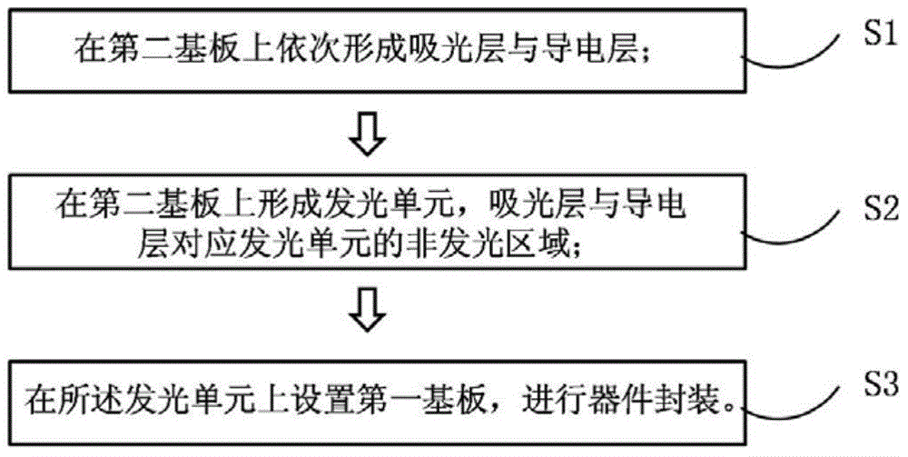
[0028] In order to make the purpose, technical solution and advantages of the present invention clearer, the following will further describe in detail the embodiments of the present invention in conjunction with the accompanying drawings.

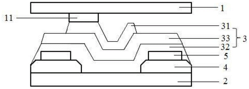
[0029] This invention may be embodied in many different forms and should not be construed as limited to the embodiments set forth herein. Rather, these embodiments are provided so that this disclosure will be thorough and complete and will fully convey the concept of the invention to those skilled in the art, and the present invention will only be defined by the appended claims. In the drawings, the size and relative sizes of layers and regions may be exaggerated for clarity. It will be understood that when an element such as a layer, region or substrate is referred to as being "formed on" or "disposed on" another element, it can be directly on the other element or present middle element. In contrast, when an element is referred to as bei...


PUM


Abstract

The invention belongs to the field of organic electroluminescence. The organic electroluminescence device comprises a first base plate, a second base plate, a plurality of lighting units, a non-lighting area corresponding to each lighting unit, light absorbing layers and conductive layers, wherein the light absorbing layers and the conductive layers are overlapped; the conductive layers are in contact connection with second conductive layers in the lighting units, so as to improve the conductive performance of a second electrode layer and lower down IR voltage drop; the light absorbing layers are arranged at the non-lighting areas and can be used for effectively reducing reflecting light of a first electrode layer, and as a result, the influence of the environmental light on the display effect can be effectively reduced. The preparation method of the organic electroluminescence device comprises the following steps: preparing the light absorbing layers, the conductive layers and the lighting units on the second base plate; buckling the first base plate on the lighting units for packing. According to the device and method, the second electrode layer of the lighting units can be directly prepared to the conductive layers and can be effectively clung to the second electrode layers, thus the risk caused by disconnection can be reduced, and the connection reliability can be improved; meanwhile, the double-board process is carried out for preparing, and therefore, the working hours can be effectively decreased, and as a result, the production efficiency can be raised.

Description

technical field [0001] The invention relates to the field of organic electroluminescence, in particular to an organic electroluminescence device capable of effectively reducing the square resistance of a cathode and a preparation method thereof. Background technique [0002] Organic electroluminescent device (English full name Organic Light Emitting Display, referred to as OLED) is an active light-emitting device, which has the advantages of high contrast, wide viewing angle, low power consumption, thinner volume, etc., and is expected to become the mainstream flat panel display technology of the next generation. It is one of the most concerned technologies in display technology. [0003] According to the light emitting direction of the organic light emitting diode in the organic electroluminescent device, the organic electroluminescent device can be divided into a bottom emission device and a top emission device. Since the light of the bottom emission device passes through...

Claims


Application Information

Patent Timeline
Patent Type & Authority Applications(China)
IPC IPC(8): H01L51/50H01L51/56H01L27/32
CPCH10K59/88H10K50/11H10K50/85H10K59/10H10K2102/302H10K71/00
Inventor 刘巍
Owner KUNSHAN GO VISIONOX OPTO ELECTRONICS CO LTD
Why Eureka
Try Eureka