Touch panel structure for avoiding metal ionization

A touch panel and metal panel technology, which is applied to semiconductor/solid-state device parts, instruments, semiconductor devices, etc., can solve the problem of large impedance value of transparent conductive film

Inactive Publication Date: 2015-03-11
INTERFACE OPTOELECTRONICS SHENZHEN +1
View PDF4 Cites 9 Cited by
  • Summary
  • Abstract
  • Description
  • Claims
  • Application Information

AI Technical Summary

Problems solved by technology

[0005] The main purpose of the present invention is to provide a technical problem aimed at solving the lack of large impedance value of the commonly used transparent conductive film

Method used


Image

  • Touch panel structure for avoiding metal ionization
  • Touch panel structure for avoiding metal ionization
  • Touch panel structure for avoiding metal ionization

Examples


Embodiment Construction

[0031] The above description about the content of the present invention and the following embodiments are used to demonstrate and explain the spirit and principle of the present invention, and provide further explanation of the patent application scope of the present invention. Regarding the characteristics, implementation and effects of the present invention, preferred embodiments are described in detail below in conjunction with the drawings.

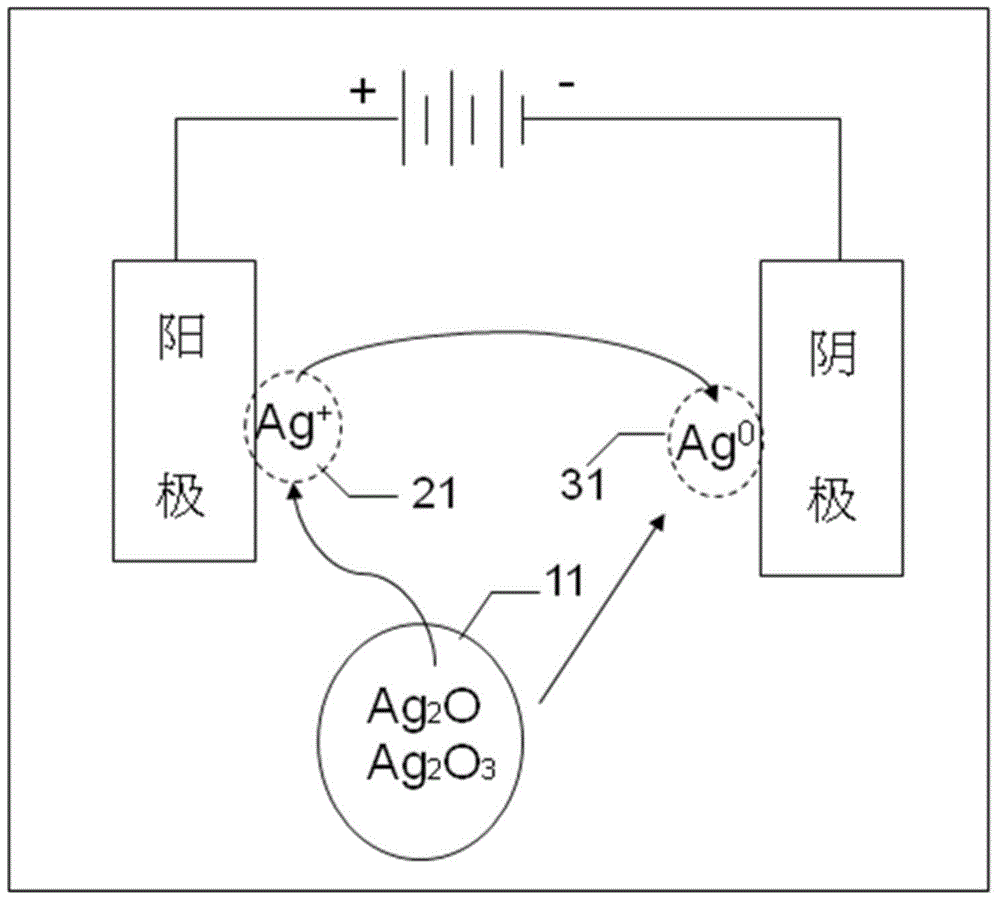
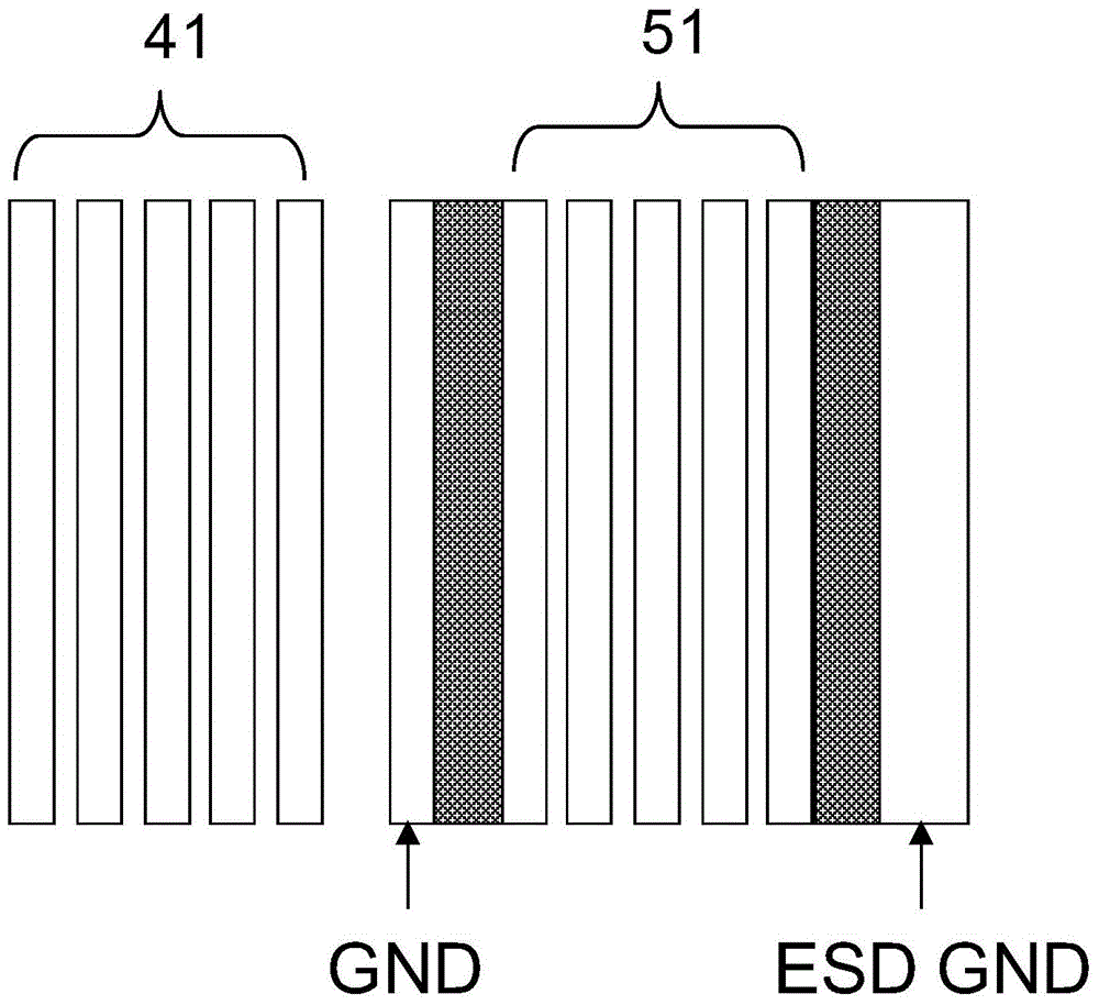
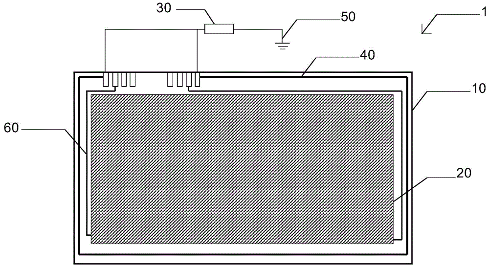
[0032] In order to facilitate understanding of the present invention, please first refer to image 3 As shown, it is a structural schematic diagram of a touch panel structure avoiding metal dissociation according to an embodiment of the present invention. As shown in the figure, the touch panel structure 1 for preventing metal dissociation disclosed in this embodiment includes a touch panel body 10, and the touch panel body 10 has a metal panel active area (Touch Panel Active Area, TPAA) ) 20. In general, the active area 20 of the me...


PUM


Abstract

The invention discloses a touch panel structure for avoiding metal ionization, and aims to solve the problem that short circuiting is caused by ionization of metal in a known metal active region. According to the touch panel structure, an original electromagnetic protective cover is designed to be directly grounded and amended to be connected to a grounding end through an electrostatic protection component. A piezoelectric resistor or a transient voltage suppressor can be selected as the electrostatic protection component. Since the electromagnetic protective cover is connected to the grounding end through the electrostatic protection component, the electromagnetic protective cover can be considered to be in an open circuit with the grounding end at ordinary times. When energy interference is produced by the outside environment, the energy can be immediately conducted to the grounding end through the electrostatic protection component, and the impedance of the electrostatic protection component is close to zero at the time, so that the energy can be quickly conducted to the grounding end at the same time to be released.

Description

technical field [0001] The invention relates to the field of touch technology, in particular to a touch panel structure for avoiding metal dissociation. Background technique [0002] At present, touch panels have been widely used in notebook computers or panels of medium and large sizes. Only by pursuing lightness and thinness can they be competitive in the market. Since size reduction is also one of the trends of today's technology, the previous stacking of glass film film (G / F / F) and double ITO layer (GF2DITO) gradually does not meet the needs of users. The development of thin and light stacking can meet the needs of the current market. For example, many materials developed at this stage can achieve the purpose of light and thin panels and reduce sheet resistance, and the use of metal mesh (Metal Mesh) is one way, which can be used to effectively replace the current transparent conductive film (ITO) The absence of large impedance values. [0003] Generally speaking, met...

Claims


Application Information

Patent Timeline
Patent Type & Authority Applications(China)
IPC IPC(8): G06F3/041G06F3/046
CPCG06F3/041G06F3/046H01L2924/0002G06F2203/04107G06F2203/04112H01L2924/00H01L23/60
Inventor 周恒生贾邦强王英琪徐安琪
Owner INTERFACE OPTOELECTRONICS SHENZHEN
Why Eureka
Try Eureka