Display panel, preparation method thereof and display device

A display panel and substrate technology, applied in nonlinear optics, instruments, optics, etc., can solve the problems of affecting the display panel picture quality, poor display panel picture quality, small display picture, etc., so as to improve the display picture quality and reduce fine bright spots Effect

Active Publication Date: 2014-07-09
BOE TECH GRP CO LTD +1
View PDF5 Cites 10 Cited by
  • Summary
  • Abstract
  • Description
  • Claims
  • Application Information

AI Technical Summary

Problems solved by technology

After the product is boxed, various processes such as thinning, polishing, and coating will be carried out to generate stress on the panel, and the spacer 4 will repeatedly rub against the alignment layer on the second substrate 2 under the action of stress. Orientation layer debris or spacer debris, these debris may move to the display area, caus

Method used


Image

  • Display panel, preparation method thereof and display device
  • Display panel, preparation method thereof and display device
  • Display panel, preparation method thereof and display device

Examples


preparation example Construction

[0053] Embodiments of the present invention also provide a method for preparing a display panel, such as Figure 5 as shown, Figure 5 It is a schematic flow chart of a method for preparing a display panel according to an embodiment of the present invention, and the method includes:

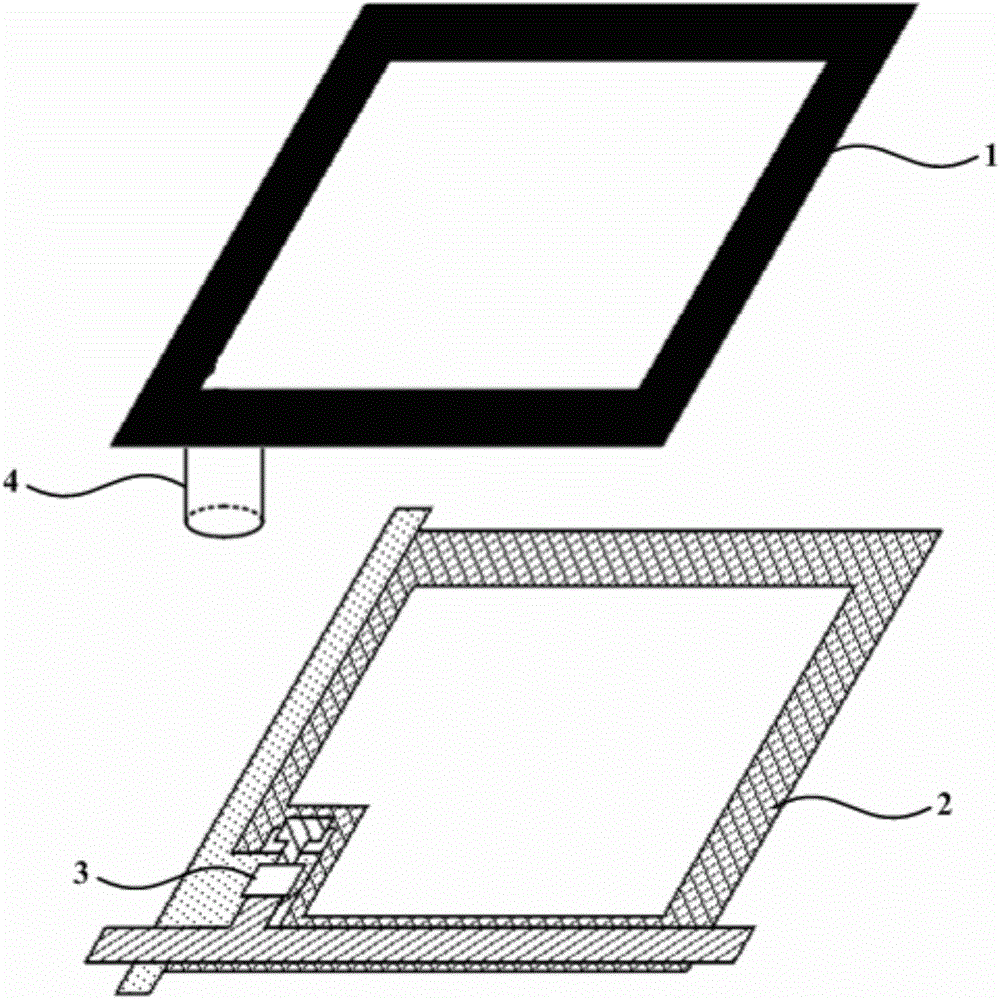
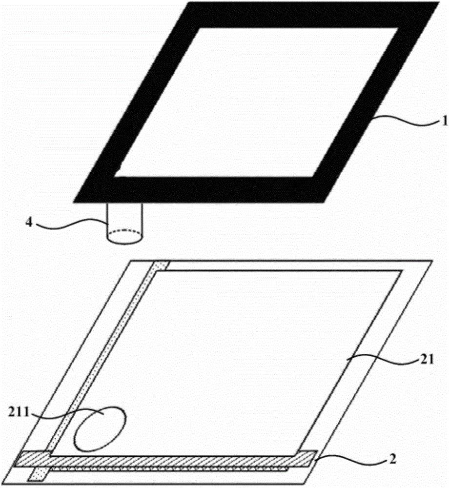
[0054] Step 101, forming at least one spacer on the first substrate;

[0055] Step 102, forming an alignment layer on the second substrate, the alignment layer having a depression corresponding to each of the spacers;

[0056] Step 103 , boxing the first substrate provided with at least one spacer and the second substrate, each of the spacers abutting against the corresponding concave portion.

[0057] Preferably, the formation of the alignment layer on the second substrate further includes:

[0058] An adhesive layer is formed within each of the recessed portions.


PUM

PropertyMeasurementUnit
Depth of depressionaaaaaaaaaa

Abstract

The invention relates to the technical field of display, and discloses a display panel and a preparation method thereof and a display device. The display panel comprises a first substrate, a second substrate and at least one spacer, wherein the first substrate and the second substrate are arranged in a combined manner, the spacers are positioned between the first and second substrates, the second substrate is provided with an alignment layer facing to the first substrate, the alignment layer is provided with recesses corresponding to all the spacers, and each spacer is fixed on the first substrate and butted in the corresponding recess. Since the alignment layer is provided with the recesses corresponding to the spaces and each spacer is butted in the corresponding recess, even the display panel generates alignment layer chips or spacer chips due to external force, the chips are retained in the recesses, and probability of diffusing to a display region is lowered; therefore, fine bright spots on the display panel are decreased, and further image quality of the display panel is improved.

Description

technical field [0001] The present invention relates to the field of display technology, in particular to a display panel, a manufacturing method thereof, and a display device. Background technique [0002] Among the flat panel display devices, Thin Film Transistor Liquid Crystal Display (TFT-LCD) has the characteristics of small size, low power consumption, relatively low manufacturing cost and low radiation, and occupies a dominant position in the current flat panel display market. leading position. [0003] Traditional LCD products such as figure 1 as shown, figure 1 It is a structural schematic diagram of a liquid crystal display panel in the prior art, figure 1 A pixel unit of a display panel is used as an illustration in the above, the liquid crystal display panel includes a first substrate 1 and a second substrate 2 placed opposite to each other, and a spacer 4 between the first substrate 1 and the second substrate 2, wherein , the first substrate 1 is a color fil...

Claims


Application Information

Patent Timeline
IPC IPC(8): G02F1/1339G02F1/1333G02F1/1337
Inventor 吴昊
Owner BOE TECH GRP CO LTD
Why Eureka
Try Eureka