Light-emitting diode-packaging structure

A technology of light-emitting diodes and packaging structures, which is applied to electrical components, electric solid-state devices, circuits, etc. It can solve the problems of difficult die bonding, wire offset, circuit breakage, etc., and achieve the effect of improving stability and increasing the active area

Active Publication Date: 2015-03-18
ZHANJING TECH SHENZHEN +1
View PDF5 Cites 1 Cited by
  • Summary
  • Abstract
  • Description
  • Claims
  • Application Information

AI Technical Summary

Problems solved by technology

However, if the area for die bonding and wire bonding is too small, it is easy to cause difficulty in die bonding or offset wire bonding, resulting in circuit breakage.

Method used


Image

  • Light-emitting diode-packaging structure
  • Light-emitting diode-packaging structure
  • Light-emitting diode-packaging structure

Examples


Embodiment Construction

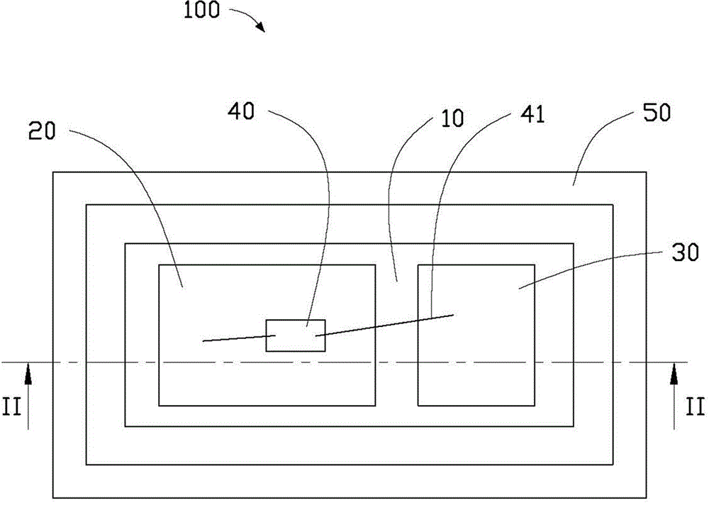
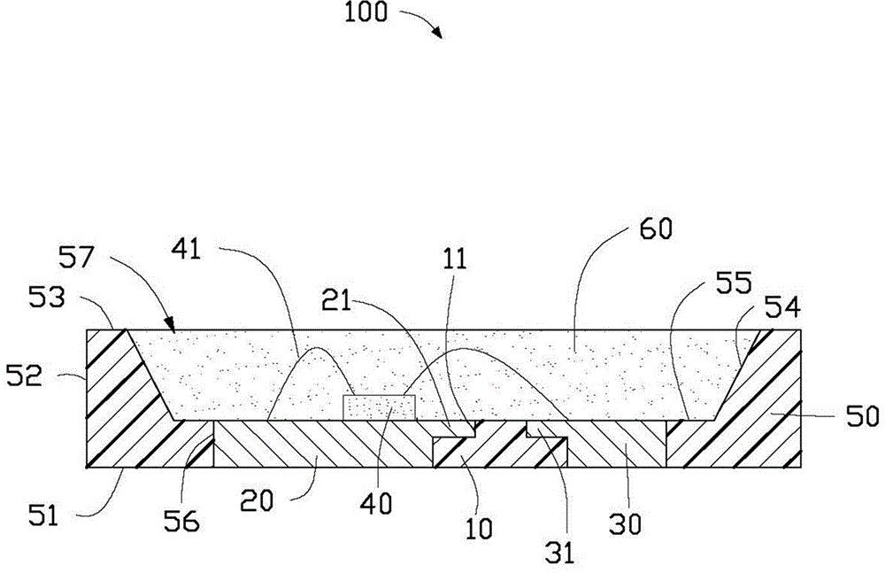
[0012] see figure 1 and figure 2 The light emitting diode packaging structure 100 according to the first embodiment of the present invention includes a substrate 10 , a first electrode 20 and a second electrode 30 located on opposite sides of the substrate 10 , a light emitting diode 40 fixed on the upper surface of the first electrode 20 , A reflective cup 50 fixed on the outer end surfaces of the first electrode 20 and the second electrode 30 and a packaging body 60 filled in the reflective cup 50 .

[0013] The substrate 10 is made of insulating material, and its longitudinal section is in an inverted T shape with a small top and a large bottom, so that two steps 11 are formed on opposite sides thereof. The substrate 10 is used to electrically isolate the first electrode 20 and the second electrode 30 .

[0014] The longitudinal section of the first electrode 20 is rectangular, and its upper end protrudes outward near an inner end surface of the substrate 10 to form a fi...


PUM


Abstract

A light emitting diode (LED) package includes a substrate, a first electrode and a second electrode mounted on opposite sides of the substrate, an LED chip mounted on a top surface of one of the electrodes and electrically connecting the first electrode and the second electrode by wire bonding, and a reflecting cup enclosing an outer periphery of the first electrode and the second electrode to expose top surfaces of the first electrode and the second electrode and bottom surfaces of the first electrode and the second electrode.

Description

technical field [0001] The invention relates to a semiconductor element, in particular to a light emitting diode packaging structure. Background technique [0002] A traditional light emitting diode packaging structure includes a substrate, a first electrode and a second electrode arranged on the upper surface of the substrate and electrically isolated from each other, a light emitting diode fixed on the first electrode, and electrically connected to the first electrode by wire bonding. , a plurality of wires of the second electrode and the light-emitting diode, and a reflective cup arranged on the first electrode and the second electrode and surrounding the light-emitting diode. The bottom surface of the reflector cup is fixed on the upper surface of the first electrode and the second electrode and extends from the edge of the first electrode and the second electrode to the area where the light emitting diode is located, thereby covering most of the first electrode and the ...

Claims


Application Information

Patent Timeline
Patent Type & Authority Applications(China)
IPC IPC(8): H01L33/48H01L33/60H01L33/52H01L33/62H01L33/64
CPCH01L33/54H01L33/486H01L33/62H01L33/60H01L2224/48257H01L2224/48247H01L2224/48091H01L2924/00014
Inventor 林厚德叶辅湘张超雄陈滨全陈隆欣
Owner ZHANJING TECH SHENZHEN
Why Eureka
Try Eureka