Liquid crystal display panel, manufacturing method thereof, and liquid display device

A liquid crystal display panel and liquid crystal display device technology, applied in nonlinear optics, instruments, optics, etc., can solve the problems of light transmittance change and uneven display of liquid crystal display devices, and achieve uniform light transmittance and thick liquid crystal cells Even, improve the effect of display unevenness

Active Publication Date: 2015-03-25
XIAMEN TIANMA MICRO ELECTRONICS +1
View PDF5 Cites 27 Cited by
  • Summary
  • Abstract
  • Description
  • Claims
  • Application Information

AI Technical Summary

Problems solved by technology

[0004] The object of the present invention is to provide a liquid crystal display panel and its manufacturing method, and a liquid crystal display device to solve the problem of light transmittance changes caused by uneven cell thickness in the existing liquid crystal display device, thereby causing uneven display in the liquid crystal display device. average phenomenon

Method used


Image

  • Liquid crystal display panel, manufacturing method thereof, and liquid display device
  • Liquid crystal display panel, manufacturing method thereof, and liquid display device
  • Liquid crystal display panel, manufacturing method thereof, and liquid display device

Examples


Embodiment 2

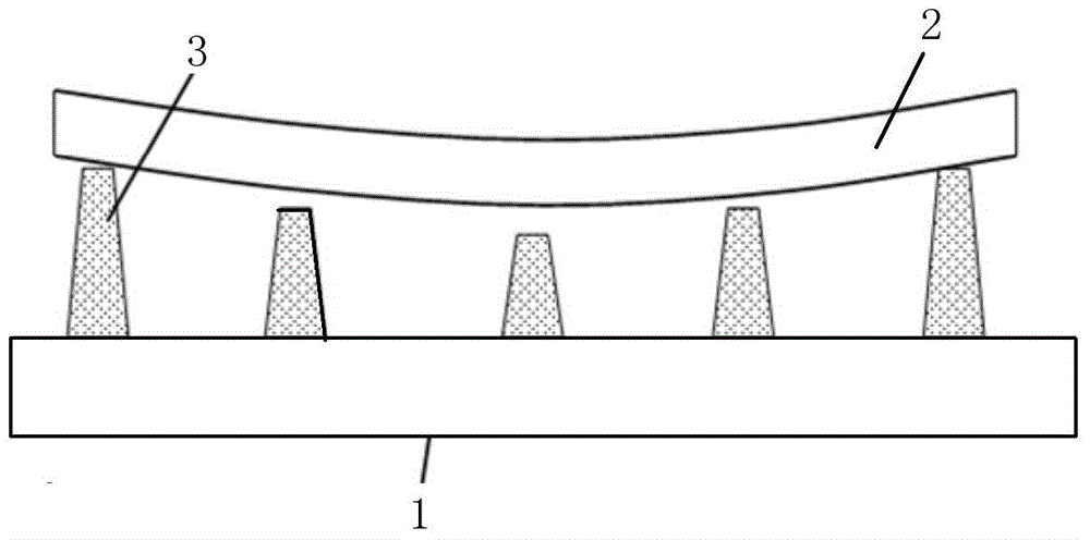
[0040] Such as Figure 4 Shown is a cross-sectional view of the liquid crystal display panel provided by Embodiment 2 of the present invention, and the supporting pillars in the liquid crystal display panel are the main supporting pillars.

[0041] Specifically, the liquid crystal display panel includes:

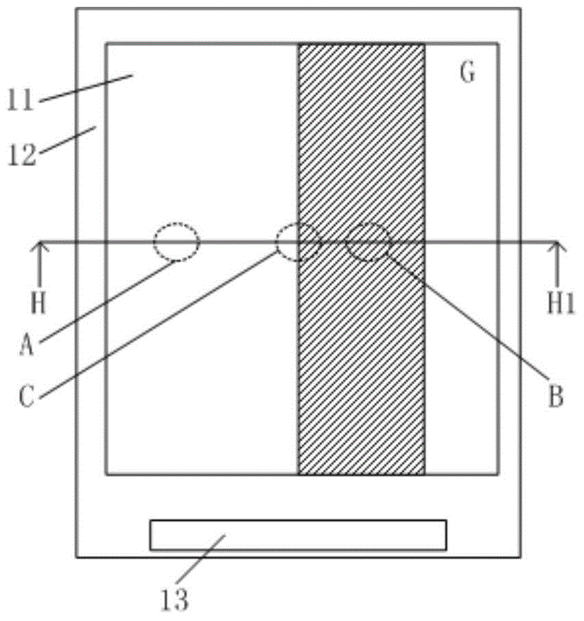
[0042] The first substrate 11, the second substrate 12 opposite to the first substrate 11, a plurality of support columns arranged between the first substrate 11 and the second substrate 12, the plurality of support columns include main support columns 17 and auxiliary support columns. Support columns 18, wherein the diameter of the main support columns 17 is greater than the diameter of the auxiliary support columns 18, the first end of each support column is connected to the first substrate 11, the thin film structure 14 arranged on the second substrate 12, the thin film structure 14 The surface of the film structure 14 is provided with a concave-convex structure, and the...

Embodiment 3

[0046] Figure 5a It is a schematic diagram of the height distribution of the prisms of the exposure machine in the production process of the liquid crystal display panel. In the process of making the support column, because the exposure energy of the prism connection part of the exposure machine is smaller than that of the normal area, generally 15mj, the exposure machine can Ultraviolet light is used for exposure, and the exposure is divided into two parts, so that the height of the support column corresponding to the prism connection part of the exposure machine is lower than the height of the support column in the normal area. Such as Figure 5a As shown, for example: in the connecting part of the exposure machine prism M4 and the exposure machine prism M5, the length of the exposure machine prism tip is 16.8mm, and the length of the exposure machine prism after removing the prism tip is 105mm. Different exposure machines There are different exposure machine prism lengths...

Embodiment 4

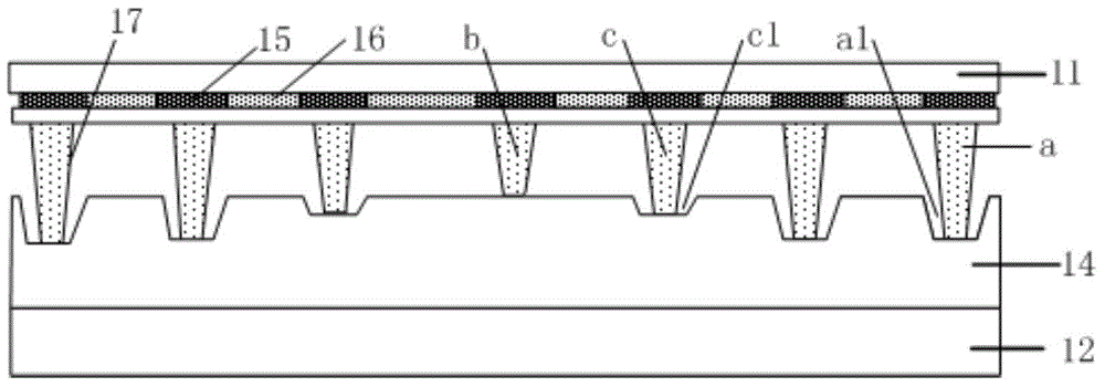
[0058] Such as Figure 8 Shown is a cross-sectional view of the liquid crystal display panel provided by Embodiment 4 of the present invention. In this embodiment, the first ends of each support column are arranged on the color filter substrate, and the second ends of the support columns are in contact with the surface of the film structure. , each support column is the same as the support column in the third embodiment of the present invention, and the difference from the third embodiment is that the film structure on the array substrate in this embodiment includes spacers with different heights, each of the spacers The surface of the mat is in contact with the second end of the main support column.

[0059] Specifically, such as Figure 5b and Figure 8 As shown, spacers with different heights can be set on the film structure 14, and the supporting columns 171 are Figure 5b The support column corresponding to the middle area E, the support column 172 is Figure 5b The s...


PUM

PropertyMeasurementUnit
thicknessaaaaaaaaaa
depthaaaaaaaaaa
thicknessaaaaaaaaaa

Abstract

The invention discloses a liquid crystal display panel, a manufacturing method of the liquid crystal display panel and a liquid display device. The liquid crystal display panel comprises a first substrate, a second substrate, a plurality of supporting pillars and a film structure, wherein the first substrate and the second substrate are arranged oppositely, the multiple supporting pillars are arranged between the first substrate and the second substrate, the first end of each supporting pillar is connected with the first substrate, the film structure is arranged on the second substrate, a concave-convex structure is arranged on the surface of the film structure, and the surface of the film structure makes contact with the second ends of the supporting pillars so that the distances between the first ends of the supporting pillars and the side, far away from the supporting pillars, of the second substrate are the same. The second ends of the supporting pillars are near the film structure. The thickness of a liquid crystal box of the liquid crystal display device is uniform, the light transmitting rate is uniform, and the phenomenon of non-uniform display of the liquid crystal display device is further solved.

Description

technical field [0001] The invention relates to the field of display technology, in particular to a liquid crystal display panel, a manufacturing method thereof, and a liquid crystal display device Background technique [0002] Thin Film Transistor Liquid Crystal Display (TFT-LCD) has become a display technology that can span all sizes due to its small size, low power consumption, and no radiation. It is widely used in fields such as TVs and notebooks. computer, monitor or mobile phone etc. [0003] Such as figure 1 as shown, figure 1 It is a structural diagram of the support column in the liquid crystal display device in the prior art. The liquid crystal display device is a liquid crystal cell formed by aligning and laminating the array substrate 2 and the color filter substrate 1 oppositely arranged. When the array substrate 2 and the color filter substrate 1 When aligning and laminating, it is necessary to use a supporting column 3 between the array substrate 2 and the...

Claims


Application Information

Patent Timeline
Patent Type & Authority Applications(China)
IPC IPC(8): G02F1/1339G02F1/1333
CPCG02F1/1333G02F1/13394G02F1/13396G02F1/13398
Inventor 文亮
Owner XIAMEN TIANMA MICRO ELECTRONICS
Why Eureka
Try Eureka