Base plate cleaning device

A technology for cleaning devices and substrates, which is applied in the manufacture of electrical components, semiconductor/solid-state devices, circuits, etc. It can solve the problems of increasing production costs, water can no longer be recycled, and cannot meet the water consumption of the primary cleaning area C, so as to reduce water consumption Quantity, the effect of reducing production costs

Active Publication Date: 2015-03-25
TCL CHINA STAR OPTOELECTRONICS TECH CO LTD
View PDF3 Cites 4 Cited by
  • Summary
  • Abstract
  • Description
  • Claims
  • Application Information

AI Technical Summary

Problems solved by technology

[0005] However, in the prior art, the cleanliness of the water after cleaning the substrate in the cleaning area A is relatively high, and because the requirements for cleaning the substrate before photolithography are high, the water after cleaning the substrate in the cleaning area A cannot be recycled for further use. In cleaning area A
In the final cleaning area E of the cleaning area after photolithography, in order to ensure the cleanliness of the substrate, pure water must be used. The primary cleaning area C and the intermediate cleaning area D are not limited to pure water, but in the prior art Among them, the circulating water after cleaning the substrate in the intermediate cleaning area D and the final cleaning area E cannot meet the water consumption of the primary cleaning area C, so it must be filled with pure water, which increases the water consumption of pure water and increases the production cost

Method used


Image

  • Base plate cleaning device
  • Base plate cleaning device
  • Base plate cleaning device

Examples


Embodiment Construction

[0021] Hereinafter, embodiments of the present invention will be described in detail with reference to the accompanying drawings. This invention may, however, be embodied in many different forms and should not be construed as limited to the specific embodiments set forth herein. Rather, the embodiments are provided to explain the principles of the invention and its practical application, thereby enabling others skilled in the art to understand the invention for various embodiments and with various modifications as are suited to particular intended uses.

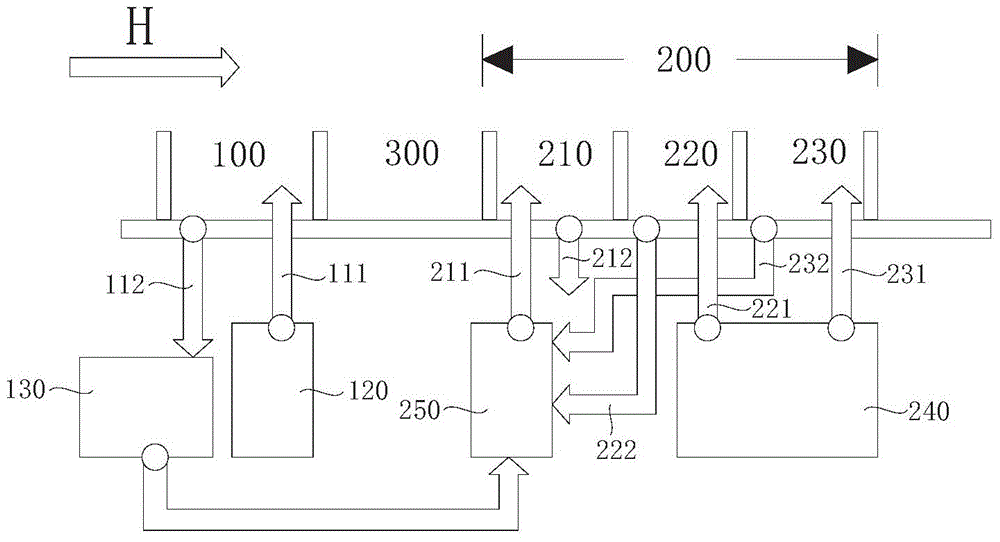
[0022] figure 2 is a schematic structural view of the substrate cleaning apparatus according to the first embodiment of the present invention.

[0023] refer to figure 2 , The substrate cleaning apparatus according to the first embodiment of the present invention includes a pre-lithography cleaning area 100 and a post-lithography cleaning area 200 . Generally, the photolithography area 300 is disposed between the pre-lit...


PUM


Abstract

The invention discloses a base plate cleaning device. The base plate cleaning device comprises a before-photoetching cleaning region (100) and an after-photoetching cleaning region (200). The before-photoetching cleaning region (100) comprises a water supply pipe and a waste discharge pipe. The water supply pipe of the before-photoetching cleaning region (100) is communicated with a first water storage device (120). The after-photoetching cleaning region (200) comprises a primary cleaning region (210), an intermediate cleaning region (220) and a terminal cleaning region (230), wherein the primary cleaning region (210), the intermediate cleaning region (220) and the terminal cleaning region (230) are sequentially and adjacently connected. The primary cleaning region (210), the intermediate cleaning region (220) and the terminal cleaning region (230) each comprise a water supply pipe and a waste discharge pipe. The water supply pipe (221) and the water supply pipe (231) of the terminal cleaning region (230) are communicated with a second water storage device (240). The water supply pipe (211) is communicated with a second recoverer (250), the waste discharge pipe (222) and the waste discharge pipe (232) are communicated with the second recoverer (250), and the second recoverer (250) are communicated with the waste discharge pipe (112). By the adoption of the base plate cleaning device, water generated after a base plate is cleaned in the before-photoetching cleaning region is recovered, the pure water consumption is reduced, and therefore production cost is reduced.

Description

technical field [0001] The invention relates to a substrate cleaning device. Background technique [0002] In the manufacturing process of the liquid crystal display device, the substrate that will form the thin film transistor (TFT) substrate needs to go through a photolithography process of coating photoresist, exposing and developing. Among them, the purpose of development is to remove the photoresist that has optically reacted during the exposure process, thereby forming a photoresist pattern corresponding to the exposure mask on the substrate. After development, the substrate is covered with photoresist. Due to the protection of the photoresist during the etching process, the metal or non-metal in the corresponding position will not be damaged, so that the purpose of forming a thin film transistor (TFT) on the substrate is finally achieved. [0003] Since the cleanliness of the substrate is very high, it is usually necessary to clean the substrate before the substrate ...

Claims


Application Information

Patent Timeline
Patent Type & Authority Applications(China)
IPC IPC(8): H01L21/02
CPCH01L21/02052H01L21/02071
Inventor 欧阳志华
Owner TCL CHINA STAR OPTOELECTRONICS TECH CO LTD
Why Eureka
Try Eureka