Supercharge Your Innovation With Domain-Expert AI Agents!

Flip Chip Package Structure

A flip-chip packaging, electrical technology, applied in electrical components, electrical solid-state devices, circuits, etc., can solve the problem of consuming human resources, increasing the frequency of manual adjustment of machine identification by operators, reducing machine driving rate and production line. work efficiency and other issues, to avoid pollution or damage and improve product quality

Active Publication Date: 2017-07-25
CHIPMORE TECH CORP LTD
View PDF4 Cites 0 Cited by
  • Summary
  • Abstract
  • Description
  • Claims
  • Application Information

AI Technical Summary

Problems solved by technology

At present, many alignment marks (alignment marks) on the tape (flip-chip package flexible circuit board) used for automatic identification of machines cannot avoid contact or friction with their packaging materials or related parts of the production machine during the production process or transportation process. As a result, the machine cannot automatically identify the alignment mark (alignment mark), and the alarm is often reported due to abnormal product quality during production, which increases the frequency of operators manually adjusting the machine identification, thereby reducing the driving rate of the machine and production line operations. Efficiency, consumes a lot of human resources

Method used


Image

  • Flip Chip Package Structure
  • Flip Chip Package Structure
  • Flip Chip Package Structure

Examples


Embodiment Construction

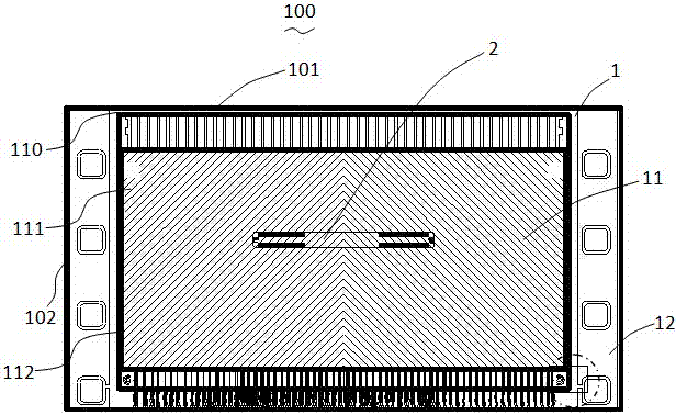
[0018] Please refer to figure 1 As shown, the present invention discloses a flip-chip packaging structure 100 , which defines that the extending direction of the long side 101 of the flip-chip packaging structure 100 is the horizontal direction, and the extending direction of the wide side 102 is the longitudinal direction. this invention figure 1 Shown is a single flip-chip packaging structure 100 , generally, several flip-chip packaging structures 100 are connected along the lateral direction and rolled up for use by panel manufacturers.

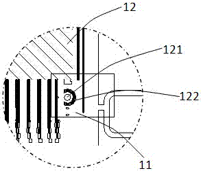
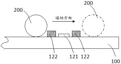
[0019] The flip-chip package structure 100 includes a flexible circuit board 1 and a chip 2 fixed on the flexible circuit board 1 . The flexible circuit board 1 is provided with an electrical functional area 11 and a non-electrical functional area 12 adjacent to the electrical functional area 11 . The electrical functional area 11 includes a base layer 110 , a circuit layer 111 disposed on the base layer 110 , and a protective layer 112 ...


PUM


Abstract

A flip-chip packaging structure, including a flexible circuit board and a chip fixed on the flexible circuit board, the flexible circuit board is provided with an electrical functional area and a non-electrical functional area adjacent to the electrical functional area, and the chip is installed In the electrical functional area to be electrically connected to the flexible circuit board, the flexible circuit board is provided with an alignment marker located in the non-electrical functional area and an alignment marker located near the alignment marker A support member, the height of the support member is greater than the height of the alignment marker. Such setting can improve the identification rate of the production machine for the alignment markers during the production process and reduce the abnormal rate of the product.

Description

technical field [0001] The invention relates to the field of electronic semiconductors, in particular to a semiconductor flip-chip packaging structure. Background technique [0002] At present, the bonding (bonding) machine of the panel factory needs to use the alignment mark (alignment mark) on the flip-chip package flexible circuit board as the alignment reference point to achieve the purpose of automatic identification of alignment production. Moreover, the ability of the machine to recognize images is limited. Therefore, the quality of the alignment mark directly affects the machine identification ability and production efficiency. At present, many alignment marks (alignment marks) on the tape (flip-chip package flexible circuit board) used for automatic identification of machines cannot avoid contact or friction with their packaging materials or related parts of the production machine during the production process or transportation process. As a result, the machine ca...

Claims


Application Information

Patent Timeline
Patent Type & Authority Patents(China)
IPC IPC(8): H01L23/544H01L23/12
Inventor 蔡文娟
Owner CHIPMORE TECH CORP LTD
Features
  • R&D
  • Intellectual Property
  • Life Sciences
  • Materials
  • Tech Scout
  • Unparalleled Data Quality
  • Higher Quality Content
  • 60% Fewer Hallucinations
Learn More