Schottky barrier diode and method for manufacturing schottky barrier diode

A Schottky barrier diode technology, which is applied in semiconductor/solid-state device manufacturing, semiconductor devices, electrical components, etc., can solve the problem of increased on-resistance, increased resistance value, and reduced contact area of ​​Schottky barrier diodes And other issues

Active Publication Date: 2015-03-25
HYUNDAI MOTOR CO LTD
View PDF5 Cites 6 Cited by
  • Summary
  • Abstract
  • Description
  • Claims
  • Application Information

AI Technical Summary

Problems solved by technology

However, due to the p+ region at the Schottky junction, the contact area between the Schottky electrode as a forward current path and the n-epitaxial layer or n-drift layer is reduced, resulting in an increase in the resistance value, and when the The on-resistance of the Schottky barrier diode increases at forward voltage

Method used


Image

  • Schottky barrier diode and method for manufacturing schottky barrier diode
  • Schottky barrier diode and method for manufacturing schottky barrier diode
  • Schottky barrier diode and method for manufacturing schottky barrier diode

Examples


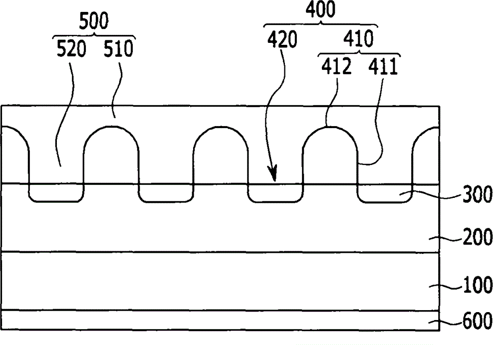
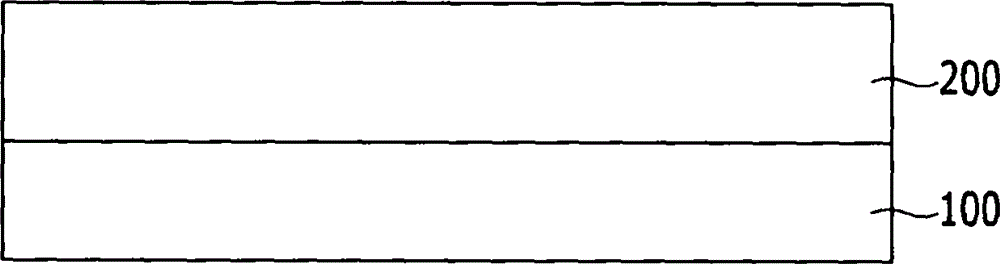
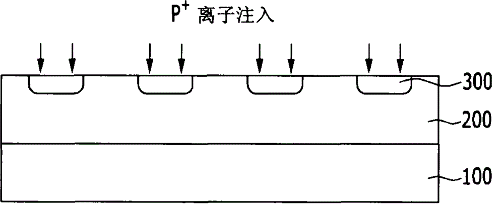
Embodiment Construction

[0027] The terminology used herein is for the purpose of describing the exemplary embodiments only and is not intended to be limiting of the invention. As used herein, the singular forms "a, an, and the" are also intended to include plural forms unless the context clearly dictates otherwise. It can also be understood that the term "comprising (comprises and / or comprising)" used in the specification refers to the existence of the described features, integers (Integer, integral), steps, operations, elements and / or parts, but does not exclude the existence of Or add one or more other features, integers, steps, operations, elements, components and / or groups thereof. As used herein, the term "and / or" includes any and all combinations of one or more of the associated listed items.

[0028] As used herein, unless otherwise stated or obvious from context, the term "about" is understood as within a range of normal tolerance in the art, for example within 2 standard deviations of the m...


PUM


Abstract

A Schottky barrier diode and a method of manufacturing the diode are provided. The diode includes an n- type epitaxial layer disposed on a first surface of an n+ type silicon carbide substrate and a plurality of p+ regions disposed within the n- type epitaxial layer. An n+ type epitaxial layer is disposed on the n- type epitaxial layer, a Schottky electrode is disposed on the n+ type epitaxial layer, and an ohmic electrode is disposed on a second surface of the n+ type silicon carbide substrate. The n+ type epitaxial layer includes a plurality of pillar parts disposed on the n- type epitaxial layer and a plurality of openings disposed between the pillar parts and that expose the p+ regions. Each of the pillar parts includes substantially straight parts that contact the n- type epitaxial layer and substantially curved parts that extend from the substantially straight parts.

Description

technical field [0001] The present invention relates to a Schottky barrier diode comprising silicon carbide (SiC) and a method for manufacturing the Schottky barrier diode. Background technique [0002] A Schottky Barrier Diode (SBD: Schottky Barrier Diode) using a Schottky junction is different from a conventional P-N diode in which a metal and a semiconductor form a junction (iunction) without using a P-N junction. This SBD exhibits fast Switching characteristics, and has lower turn-on voltage characteristics than P-N diodes. [0003] A conventional Schottky barrier diode uses a p+ region to form a junction barrier Schottky (JBS: Junction Barrier Schottky) structure at the lower end of the Schottky junction to reduce leakage current, thereby reducing the leakage current by making the When the voltage is high, the diffused P-N junction depletion layer overlaps to obtain the effect of blocking leakage current and improve the breakdown voltage. However, due to the p+ region...

Claims


Application Information

Patent Timeline
Patent Type & Authority Applications(China)
IPC IPC(8): H01L29/872H01L21/329
CPCH01L29/06H01L29/66143H01L29/872H01L29/0619H01L29/1608H01L29/6606
Inventor 郑永均千大焕洪坰国李钟锡朴正熙
Owner HYUNDAI MOTOR CO LTD
Why Eureka
Try Eureka