NOR flash memory and manufacture method thereof

A manufacturing method and technology of flash memory, applied in the direction of electrical components, electric solid devices, circuits, etc., can solve the problems of inability to eliminate the mutual interference of flash memory cells, increase the coupling of flash memory cells, and large floating gate area, so as to achieve a large erasing effect The effect of reading current, reducing resistance, and increasing junction area

Active Publication Date: 2019-05-07
SHANGHAI HUALI MICROELECTRONICS CORP
View PDF3 Cites 1 Cited by
  • Summary
  • Abstract
  • Description
  • Claims
  • Application Information

AI Technical Summary

Problems solved by technology

However, due to the large physical thickness of high-dielectric materials, while increasing the coupling rate of flash memory cells, it will increase the coupling between adjacent flash memory cells and increase the crosstalk of flash memory
Moreover, the floating gate area of ​​the fin structur

Method used


Image

  • NOR flash memory and manufacture method thereof
  • NOR flash memory and manufacture method thereof
  • NOR flash memory and manufacture method thereof

Examples


Example Embodiment

[0065] Manufacturing method of existing NOR flash memory:

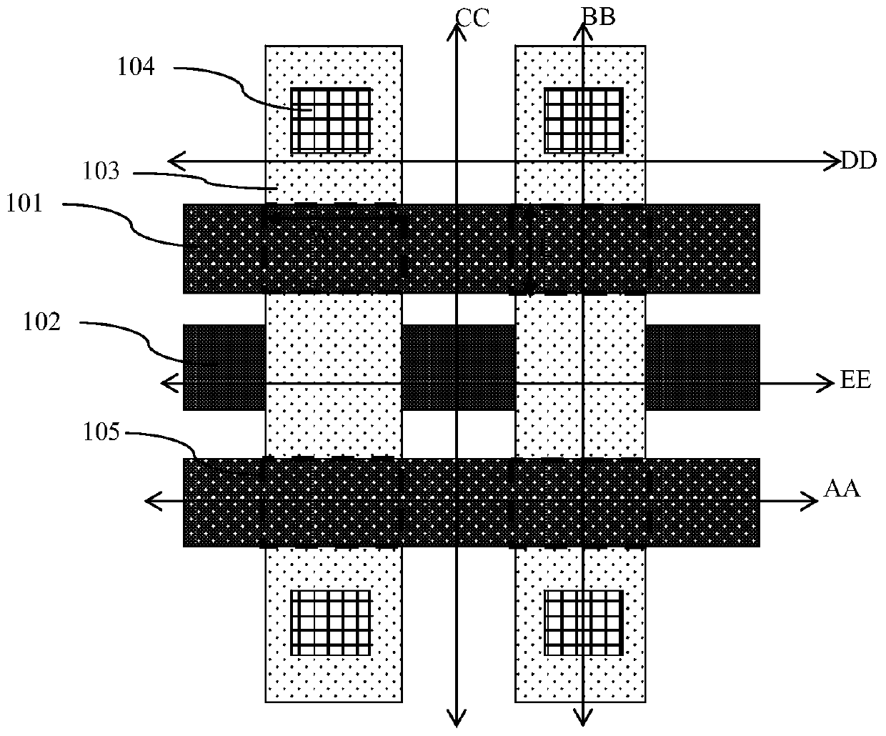
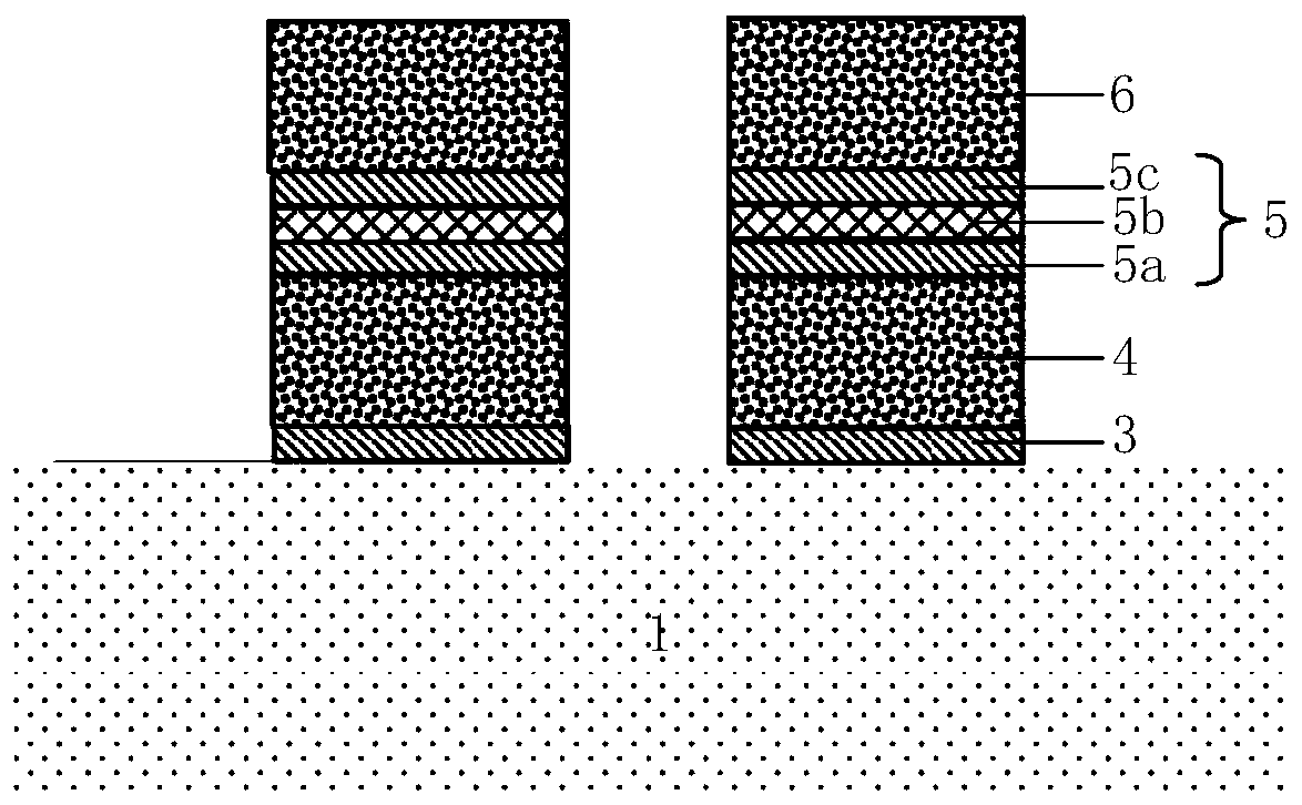
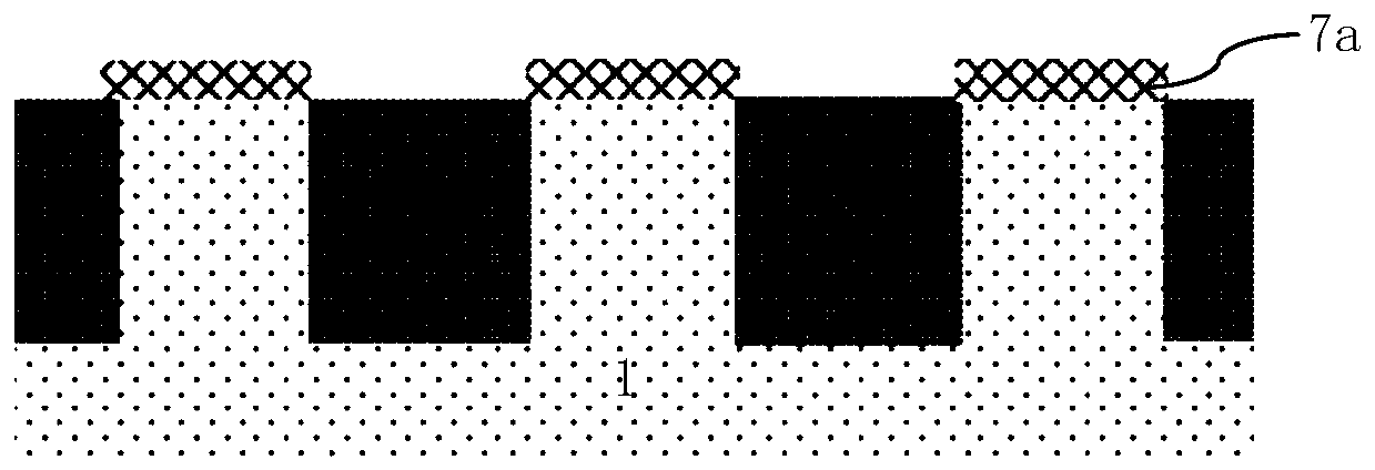
[0066] Such as figure 1 Shown is the layout structure of the storage area of ​​the existing NOR flash memory; Figure 2A It is the back edge of gate structure formation in the existing NOR flash memory manufacturing method figure 1 Sectional view of line BB; Figure 2B It is the source and drain injection timing in the existing NOR flash memory manufacturing method figure 1 Sectional view of line DD; Figure 2C It is the source and drain injection timing in the existing NOR flash memory manufacturing method figure 1 The cross-sectional view of the middle EE line; the existing manufacturing method of NOR flash memory includes the following steps:

[0067] Step 1: Provide a semiconductor substrate 1, form a field oxygen 2 in the semiconductor substrate 1 and isolate the active region 103 by the field oxygen 2.

[0068] In the existing method, the semiconductor substrate 1 is a silicon substrate.

[0069] Generally, the field oxy...


PUM


Abstract

The invention discloses a NOR flash memory. In the flash cell array of the storage area of the NOR flash memory, active regions are in strip shapes and are arranged in parallel. The polycrystalline silicon of polycrystalline silicon control gates of the flash cells in the same row are connected together to form a polycrystalline silicon row. A polycrystalline silicon floating gate is on top of theactive region perpendicularly intersecting the polycrystalline silicon row and is isolated by a first gate oxide layer. A drain region comprises a self-aligned conformal injection region extending tothe sides of the active regions. The position of the self-aligned conformal injection region is defined by the self-aligned etched back field oxygen. The self-aligned etch back region of the field oxide is formed by the self-aligned definition of the gate structure and the active region after the gate structure etching. In the source region, a self-aligned conformal injection region is also superimposed. The invention also discloses a method for manufacturing a NOR flash memory. The NOR flash memory can improve the programming efficiency without changing the gate structure, and can also reduce electric leakage and improve the performance of the device.

Description

technical field [0001] The invention relates to the field of semiconductor integrated circuits, in particular to a NOR flash memory (Flash), and also relates to a manufacturing method of the NOR flash memory. Background technique [0002] Flash memory has been widely used as the best choice for non-volatile memory applications due to its advantages of high density, low price, and electrical programmability and erasability. At present, flash memory cells are mainly implemented at the 65nm technology node. With the demand for large-capacity flash memory, the number of chips on each silicon wafer will be reduced by using the existing technology nodes. At the same time, the increasing maturity of new technology nodes also promotes the production of flash memory cells with high-node technologies. [0003] Existing flash memory cells usually use hot electron injection to achieve programming. Hot electron injection is to turn on the channel by applying high voltage to the gate, an...

Claims


Application Information

Patent Timeline
IPC IPC(8): H01L27/11517H01L27/11521
Inventor 田志李娟娟陈昊瑜邵华
Owner SHANGHAI HUALI MICROELECTRONICS CORP
Why Eureka
Try Eureka