Novel high-current-density fast recovery diode structure and manufacturing method thereof

A technology with high current density and recovery diodes, which is applied in the manufacture of circuits, electrical components, semiconductors/solid-state devices, etc., can solve limited problems, increase economic benefits, increase device junction area, and reduce device active area area Effect

Active Publication Date: 2015-07-22
BEIJING MXTRONICS CORP +1
View PDF4 Cites 1 Cited by
  • Summary
  • Abstract
  • Description
  • Claims
  • Application Information

AI Technical Summary

Problems solved by technology

[0006] The technical problem solved by the present invention is: to overcome the deficiencies of the existing technology, to provide a new type of high current density fast recovery diode structure and its manufacturing method, by digging grooves on the front of the chip, and then depositing boron-doped polysilicon to push the junction to form the anode region of the device. The grooved anode region is formed, which effectively solves the problem of limited current density of the conventional planar junction structure and improves the current density of the device

Method used


Image

  • Novel high-current-density fast recovery diode structure and manufacturing method thereof
  • Novel high-current-density fast recovery diode structure and manufacturing method thereof
  • Novel high-current-density fast recovery diode structure and manufacturing method thereof

Examples


Embodiment Construction
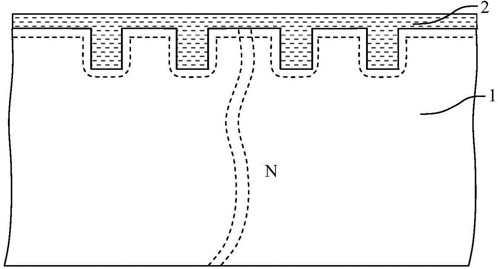
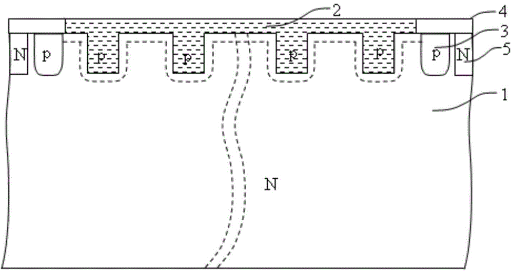
[0028] The basic idea of ​​the present invention is to provide a new type of high current density fast recovery diode structure, aiming at the problems of relatively low current density and low current capacity of the existing conventional planar junction devices, through trenching technology combined with boron-doped polysilicon deposition The formation of the grooved anode region can significantly increase the junction area of ​​the anode active region compared with the conventional planar structure, increase the current density of the device, save the chip area and improve economic benefits under the same current. Heavily doped polysilicon can form a good ohmic contact with the N-type substrate, improving device reliability.

[0029] The present invention will be described in further detail below in conjunction with the accompanying drawings.

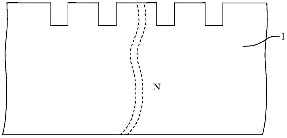
[0030] like figure 1 and Figure 4 As shown, a new type of high current density fast recovery diode structure, including (1) N-ty...


PUM


Abstract

The invention discloses a novel high-current-density fast recovery diode structure and a manufacturing method thereof, is applicable to the production of large-current fast recovery diodes, and belongs to the field of semiconductor devices. The method is characterized in that the grooving technology is used, grooves are formed in the active area on the front side of a chip, groove intervals are correspondingly adjusted according to device performance parameters, boron-doped polycrystalline silicon is then used for deposition, and a device grooved anode area is formed through pushing; a method using vacuum platinum steaming before annealing is used on the back of a single chip, and good central fast recovery feature is achieved; a terminal area is consistent with a conventional device and adopts a field ring structure; compared with the prior art, the novel high-current-density fast recovery diode structure can evidently increase device current density in unit chip area and increase device current capacity; the device active area of devices with identical current indexes can be effectively reduced, wafer utilization rate is increased, and economic benefits are increased; the heavily-doped polycrystalline silicon can be in ohmic contact with an N-type chip, and device reliability is increased.

Description

technical field [0001] The invention relates to a novel high current density fast recovery diode structure and its manufacturing method, which belongs to the technical field of power semiconductor devices. Background technique [0002] Fast recovery diodes are widely used in pulse width modulators, switching power supplies, uninterruptible power supplies, etc. In the device, it is used for high-frequency, high-voltage, high-current rectification, freewheeling and protection, and has become an indispensable part of the application device. [0003] The research and development of power semiconductor devices has led to the continuous development of fast recovery diodes in the direction of large capacity, high frequency, high efficiency, high reliability and lower cost. [0004] In the manufacture of fast recovery diodes, the method to reduce the reverse recovery time is to introduce recombination centers inside the device. Currently widely used technical means are light ion i...

Claims


Application Information

Patent Timeline
Patent Type & Authority Applications(China)
IPC IPC(8): H01L29/861H01L21/329H01L29/06
CPCH01L29/0615H01L29/6609H01L29/8613
Inventor 姚全斌赵元富吴立成王传敏殷丽王成杰赵昕张文敏冯幼明
Owner BEIJING MXTRONICS CORP
Why Eureka
Try Eureka