High level integration phase change memory device having an increased diode junction area and method for manufacturing the same

a phase change memory and diode junction technology, applied in semiconductor devices, digital storage, instruments, etc., can solve the problems of difficult if not impossible to achieve a high level of integration of drams, volatile rams (random access memory) end up losing inputted information, flash memory devices also suffer from difficulty if not impossible to achieve a high level of integration

Active Publication Date: 2010-05-13
SK HYNIX INC
View PDF8 Cites 1 Cited by
  • Summary
  • Abstract
  • Description
  • Claims
  • Application Information

AI Technical Summary

Benefits of technology

[0011]Embodiments of the present invention are directed to a phase change memory device that can increase a junction area between an N-type area and a P-type area in PN diodes as cell switching elements, and a method for manufacturing the same.

Problems solved by technology

The volatile RAMs (random access memory) end up losing their inputted information when the power is interrupted.
To this end, since the surface area of an electrode must be increased, it is difficult if not impossible to accomplish a high level of integration of DRAMs.
Further, with regards to flash memory devices, because these devices comprise two stacked gates, a high operation voltage is required and often times a separate booster circuit is needed to generate the necessary operation voltage for writing and deletion operations.
Likewise, flash memory devices also suffer from being difficult if not impossible to accomplish a high level of integration.
However, these types of conventional vertical PN diodes suffer a problem when highly integrating these devices in that their junction areas between an N-type area and a P-type area become too small which means that their operating currents decrease.
Even though the junction area between the N-type area and the P-type area can be increased by simply increasing the size of the N-type epi-silicon, the degree of integration is correspondingly adversely influenced in this case.

Method used


Image

  • High level integration phase change memory device having an increased diode junction area and method for manufacturing the same
  • High level integration phase change memory device having an increased diode junction area and method for manufacturing the same
  • High level integration phase change memory device having an increased diode junction area and method for manufacturing the same

Examples


Embodiment Construction

[0058]Hereafter, the specific embodiments of the present invention will be described in detail with reference to the accompanying drawings.

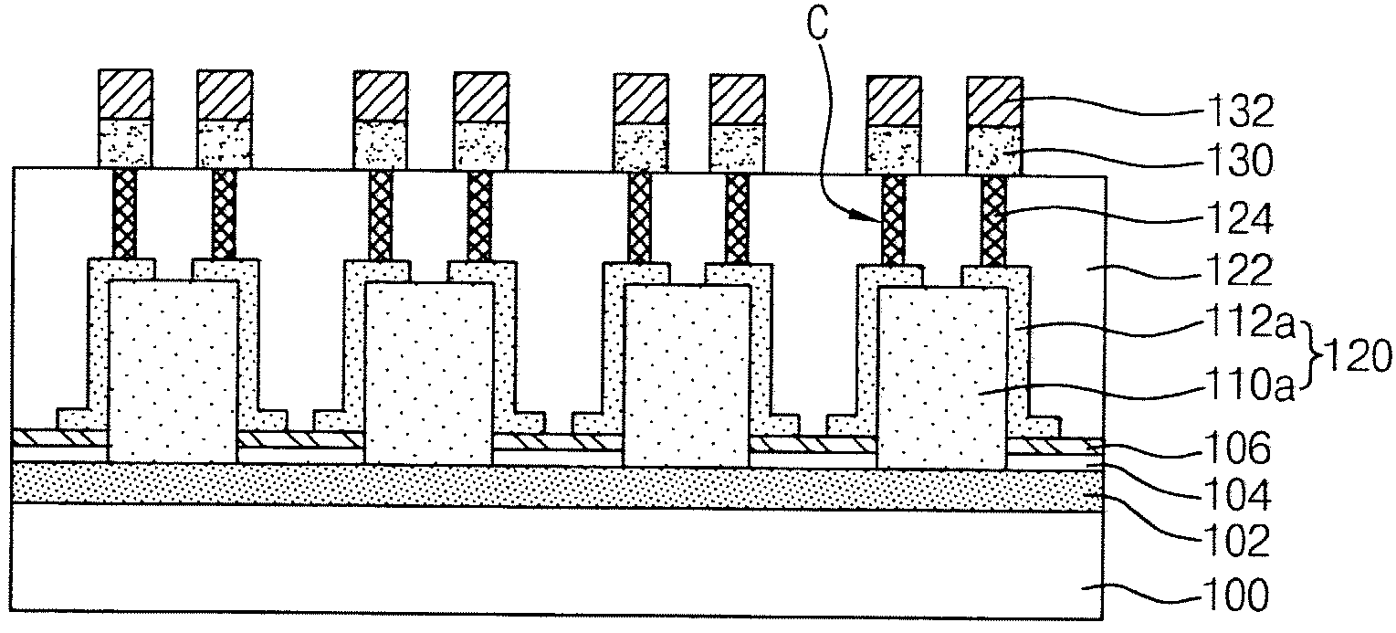
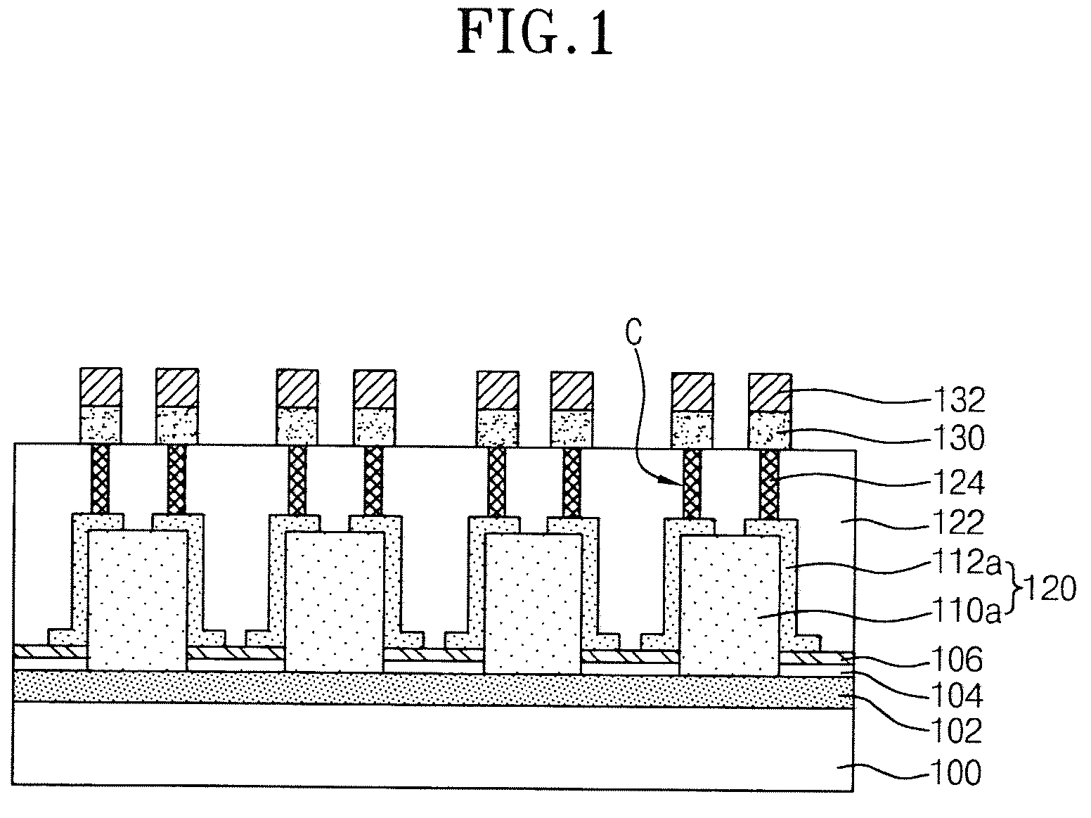
[0059]FIG. 1 is a sectional view illustrating a phase change memory device in accordance with an embodiment of the present invention.

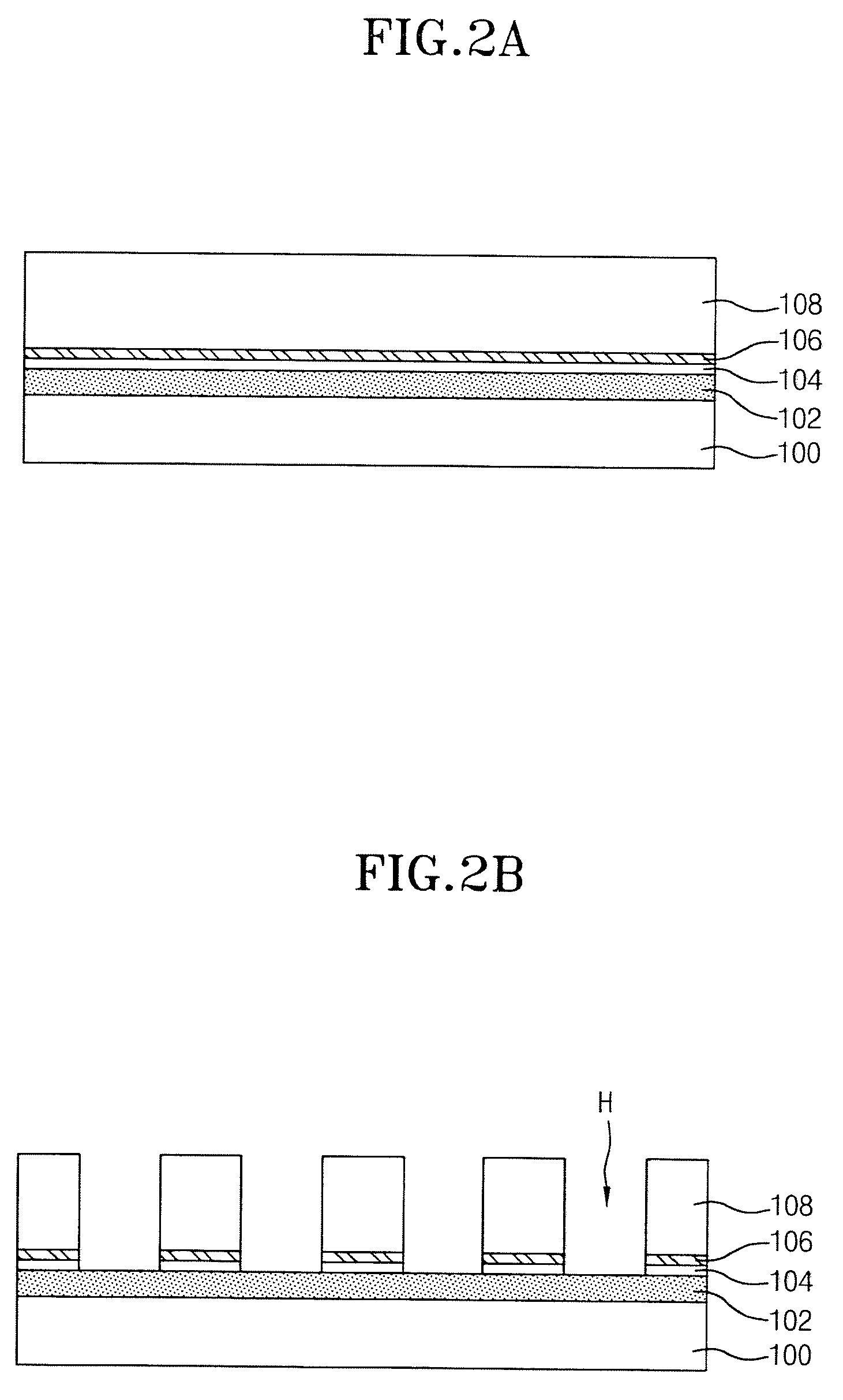
[0060]Referring to FIG. 1, a first conductivity type high concentration area, that is, an N+ base area 102, into which N-type impurities are ion-implanted at a high concentration, is formed in the surface of a semiconductor substrate 100. The semiconductor substrate 100 has a bar type active region. It is preferred that the N+ base area 102 be understood as being formed in the surface of the active region. The N+ base area 102 has an impurity concentration of, for example, between about 1×10²⁰˜1×10²² ions / cm3.

[0061]First conductivity type silicon pillars, that is, N-type silicon pillars 110a, which are doped with N-type impurities, are formed in the active region of the semiconductor substrate 100 which is formed wi...


PUM


Abstract

A phase change memory device includes a semiconductor substrate active region, a plurality of first conductivity type silicon pillars, and a plurality of second conductivity type silicon patterns. The plurality of first conductivity type silicon pillars is formed on the semiconductor active region such that each first conductivity type silicon pillar is provided for two adjoining cells. The plurality of second conductivity type silicon patterns is formed on the plurality of first conductivity type silicon pillars such that two second conductivity type silicon patterns are formed on opposite sidewalls of each first conductivity type silicon pillars. Two adjoining cells together share only one first conductivity type silicon pillar and each adjoining cell is connected to only one second conductivity type silicon pattern which constitutes a PN diode which serves as a single switching element for each corresponding cell.

Description

CROSS-REFERENCE TO RELATED APPLICATIONS[0001]The present application claims priority to Korean patent application number 10-2008-0111265 filed on Nov. 10, 2008, which is incorporated herein by reference in its entirety.BACKGROUND OF THE INVENTION[0002]The present invention relates to a phase change memory device and a method for manufacturing the same, and more particularly, to a phase change memory device which can increase a junction area between an N-type area and a P-type area when forming PN diodes as cell switching elements and a method for manufacturing the same.[0003]In general, memory devices are largely divided into two groups. The volatile RAMs (random access memory) end up losing their inputted information when the power is interrupted. In contrast, non-volatile ROMs (read-only memory) can continuously maintain their stored state of inputted information even when power is interrupted. As among volatile RAMs, the DRAM (dynamic RAM) and the SRAM (static RAM) are well known...

Claims


Application Information

Patent Timeline
Patent Type & Authority Applications(United States)
IPC IPC(8): H01L29/04H01L21/329
CPCH01L27/2409H01L29/685H01L45/06H01L45/1233H01L45/126H01L45/144H01L45/165H01L45/1675H10B63/20H10N70/8413H10N70/231H10N70/043H10N70/8828H10N70/063H10N70/826H10N70/8825
Inventor KIM, KYUNG DO
Owner SK HYNIX INC
Why Eureka
Try Eureka