Three-terminal atom switching device and preparing method thereof

A technology of switching devices and atoms, which is applied in the field of microelectronics, can solve the problems of large leakage current, low switching, and increase the difficulty of designing non-linear resistance at both ends, so as to reduce the difficulty of design

Active Publication Date: 2015-03-25
INST OF MICROELECTRONICS CHINESE ACAD OF SCI
View PDF15 Cites 11 Cited by
  • Summary
  • Abstract
  • Description
  • Claims
  • Application Information

AI Technical Summary

Problems solved by technology

[0005] The switching ratio of the non-linear resistors reported at both ends is generally low, the leakage current is large, and the transition voltage of the thre

Method used


Image

  • Three-terminal atom switching device and preparing method thereof
  • Three-terminal atom switching device and preparing method thereof
  • Three-terminal atom switching device and preparing method thereof

Examples


Example Embodiment

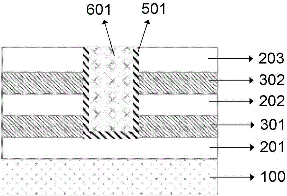
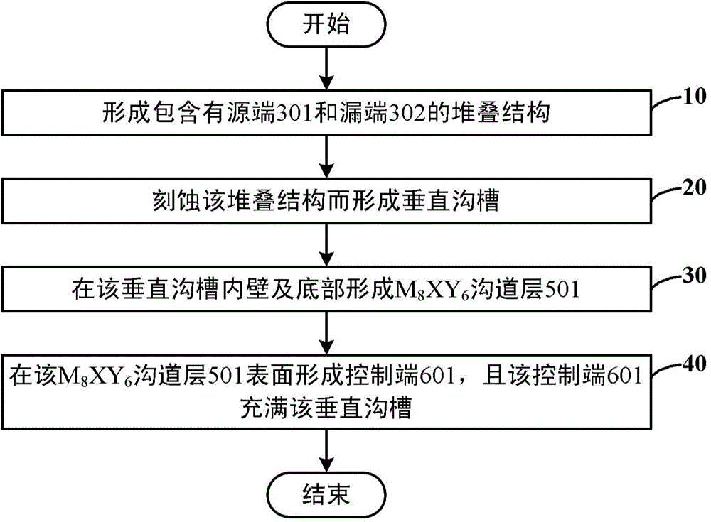
[0042] Hereinafter, the present invention will be more fully described in reference embodiments in conjunction with the drawings. The present invention provides preferred embodiments, but should not be considered as limited to the embodiments set forth herein. In the figure, the thickness of the layers and regions are enlarged for clarity, but as a schematic diagram, it should not be regarded as strictly reflecting the proportional relationship of geometric dimensions. The reference figure here is a schematic diagram of an idealized embodiment of the present invention. The embodiment shown in the present invention should not be considered as limited to the specific shape of the area shown in the figure, but includes the resulting shape. It is illustrative, but this should not be considered as limiting the scope of the invention.

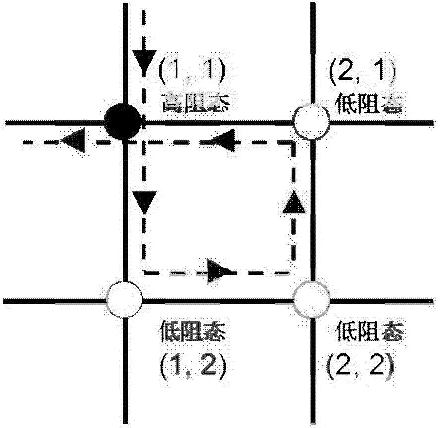
[0043] The present invention is based on a three-terminal atomic switch device, which relies on the highly non-linear change characteristics of the res...


PUM

PropertyMeasurementUnit
Thicknessaaaaaaaaaa
Thicknessaaaaaaaaaa

Abstract

The invention discloses a three-terminal atom switching device and a preparing method thereof, and belongs to the technical field of microelectronic manufacturing and memorizers. The three-terminal atom switching device comprises a stacking structure comprising a source end and a drain end, a vertical groove formed by etching the stacking structure, an M8XY6 channel layer formed on the inner wall and the bottom of the vertical groove, and a control end formed on the surfaces of the M8XY6 channel layer, the vertical groove is full of the control end, and a source end resistor and a drain end resistor are regulated through the control end. On the basis of the three-terminal atom switching device, the high switching ratio characteristic is achieved in the height nonlinearity changing characteristic of the resistance between the source end and the drain end along with the voltage of the control end, the structure is simple, integration is easy, density is high, cost is low, the three-terminal atom switching device can be applied to a gating tube of a cross array structure, and the crosstalk phenomenon caused by leakage current is restrained. The three-terminal atom switching device is also suitable for a plane stacking cross array structure and a vertical cross array structure, and the high-density three-dimensional storage is achieved.

Description

Technical field [0001] The invention relates to the technical field of microelectronics, in particular to a three-terminal atomic switch device suitable for passive cross-array integrated gate tubes and a preparation method thereof. Background technique [0002] Resistive memory, such as resistive random access memory, phase change memory, and magnetic memory, has received high attention at home and abroad due to its excellent characteristics in cell area, three-dimensional integration, low power consumption, high erasing speed and multi-value storage. . [0003] The array architecture of resistive random access memory can be divided into passive cross array and active array. In the passive cross array, each memory cell is determined by the upper and lower electrodes formed by intersecting word lines and bit lines. The smallest memory cell area can be achieved in a planar structure-4F 2 , Where F is the characteristic size. Since the passive cross array does not depend on the pre...

Claims


Application Information

Patent Timeline
IPC IPC(8): H01L45/00
Inventor 吕杭炳刘明刘琦龙世兵
Owner INST OF MICROELECTRONICS CHINESE ACAD OF SCI
Why Eureka
Try Eureka