
Eureka
For R&D, Eureka makes reading and utilizing patents & technical documents easy.
Eureka AIR
Designed for self-driven R&D workflows. Generate viable solutions, solve complex R&D challenges, empower your innovation with AI.

Eureka Materials
Designed for material experts only. Revolutionize your material R&D, from search, analyze, to developing new materials.

TechResearch
Generate reliable direction feasibility study reports for your R&D in just a few steps.

TechSeek
Discover and master advanced knowledge NOW. Basics, ideas, possibilities, all at once.

TechMind
As an expert in R&D Theories, TechMind can generates customized viable solutions instantly.

TechRisk
Analyze your overall solution with one click, know your potential R&D risks in advance.

TechMonitor
Get weekly tech updates, stay abreast of the latest tech innovations and key insights.
Charged particle multi-beamlet lithography system and cooling arrangement manufacturing method
A charged particle beamlet, charged particle technology, applied in circuits, discharge tubes, electrical components, etc., can solve problems such as reduced pattern accuracy
- Summary
- Abstract
- Description
- Claims
- Application Information
AI Technical Summary
Problems solved by technology
Method used
Image

Examples
Embodiment Construction
[0035] The following is a description of various embodiments of the invention, given by way of example only, with reference to the accompanying drawings.
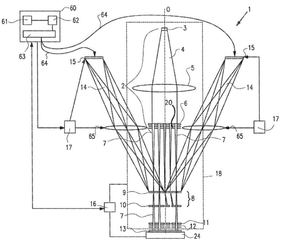
[0036] figure 1 A simplified schematic embodiment of an embodiment of a charged particle lithography apparatus 1 is shown. Such lithographic systems are described, for example, in U.S. Patent Nos. 6,897,458 and 6,958,804 and 7,019,908 and 7,084,414 and 7,129,502, U.S. Patent Application Publication No. 2007 / 0064213, and Serial Nos. 61 / 031,573 and 61 As described in co-pending applications No. / 031,594 and 61 / 045 / 243 and 61 / 055,839 and 61 / 058,596 and 61 / 101 / 682, which are assigned in their entirety to all of the present invention are incorporated herein by reference in their entirety.
[0037] exist figure 1 In the embodiment shown in , the lithographic apparatus 1 comprises a beamlet generator 2 for generating a plurality of beamlets, a beamlet modulator 8 for patterning the beamlets to form modulated beamlets, and a beam...
PUM
 Abstract
Description
Claims
Application Information
 - R&D Engineer
- R&D Manager
- IP Professional
- Industry Leading Data Capabilities
- Powerful AI technology
- Patent DNA Extraction
Browse by: Latest US Patents, China's latest patents, Technical Efficacy Thesaurus, Application Domain, Technology Topic, Popular Technical Reports.
© 2024 PatSnap. All rights reserved.Legal|Privacy policy|Modern Slavery Act Transparency Statement|Sitemap|About US| Contact US: help@patsnap.com